 12
12
ZOTAC GeForce RTX 3090 AMP Extreme Holo Review
Test Setup »High-resolution PCB Pictures
These pictures are for the convenience of volt modders and people who would like to see all the finer details on the PCB. Feel free to link back to us and use these in your articles, videos or forum posts.

High-res versions are also available (front, back).
Circuit Board (PCB) Analysis
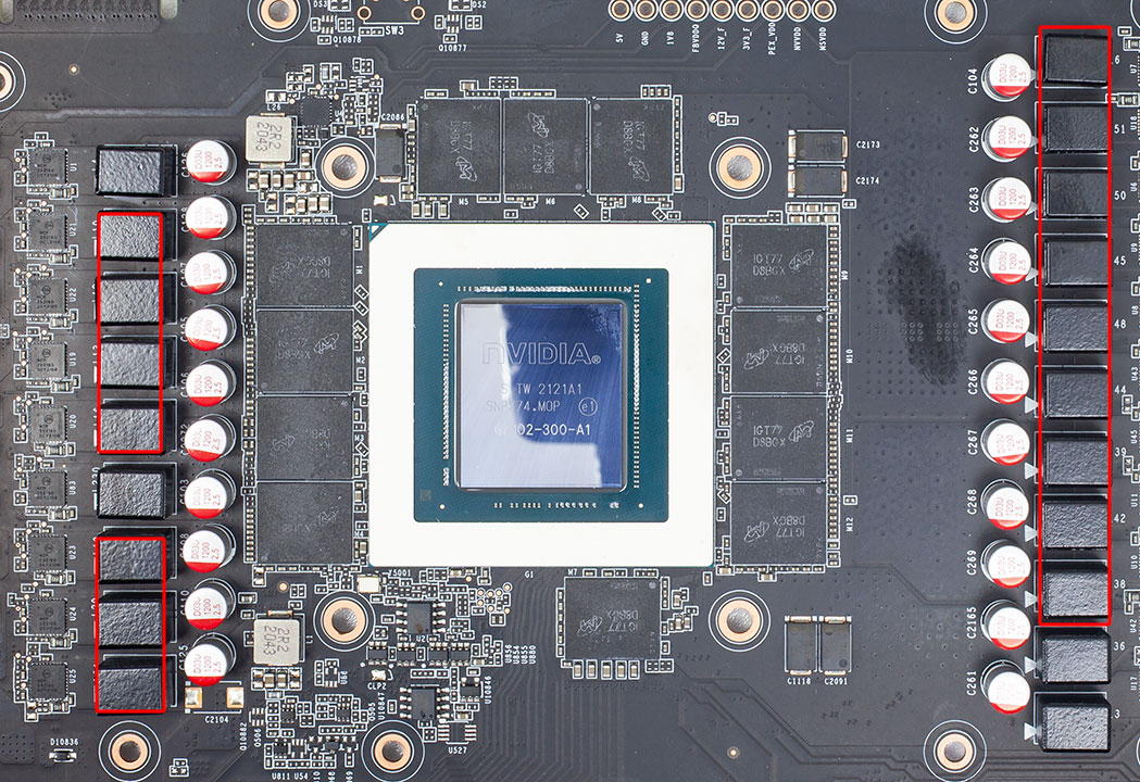


The GPU VRM is 16-phase, controlled by two UPI uP9511R voltage controllers.

The GPU VRM uses OnSemi NCP252160 DrMOS components rated for 60 A.


Memory is a four-phase design controlled by another UPI uP9511R controller.

The memory VRM uses the same 60 A OnSemi NCP252160 DrMOS components as the GPU VRM.

The GDDR6X memory chips are made by Micron and carry the model number D8BGX, which decodes to MT61K256M32JE-21. They are specified to run at 1313 MHz (21 Gbps GDDR6X effective).

NVIDIA's GA102 graphics processor is the company's second Ampere architecture chip; the first one targeted at GeForce gamers. It is produced on a 8 nanometer process at Samsung and has a transistor count of 28 billion with a die size of 628 mm².
Jun 5th, 2024 05:48 EDT
change timezone
Latest GPU Drivers
New Forum Posts
- Zen5 only 16 core. (62)
- 9900X3D - Will AMD solve the split CCD issue (2)
- Can I move Windows 11 pro licence into virtual machine? (21)
- Need Help Choosing a Laptop for Occasional Use While Traveling (Graphic Design, Photoshop) (0)
- X570 TUF User Profiles (3)
- Post your SilverBench multi-core result (11)
- The TPU Darkroom - Digital SLR and Photography Club (3959)
- AsRock Deskmeet X600 release date is close... (15)
- [Help] New (used) 10700 not working? (1)
- Decent, lightweight alternative to Windows Mail? (29)
Popular Reviews
- Intel Lunar Lake Technical Deep Dive - So many Revolutions in One Chip
- Kioxia Exceria Plus G3 2 TB Review
- NZXT H6 Flow RGB Review
- Corsair iCUE XC7 RGB Elite LCD CPU Water Block Review
- SilverStone KL07E Review
- Upcoming Hardware Launches 2024 (Updated May 2024)
- NuPhy Air96 V2 Low Profile Wireless Mechanical Keyboard Review
- AMD Ryzen 7 7800X3D Review - The Best Gaming CPU
- Ghost of Tsushima Performance Benchmark Review - 35 GPUs Tested
- ASUS GeForce RTX 4060 Dual OC Review - The Best RTX 4060
Controversial News Posts
- NVIDIA to Only Launch the Flagship GeForce RTX 5090 in 2024, Rest of the Series in 2025 (154)
- AMD Hits Highest-Ever x86 CPU Market Share in Q1 2024 Across Desktop and Server (140)
- AMD RDNA 5 a "Clean Sheet" Graphics Architecture, RDNA 4 Merely Corrects a Bug Over RDNA 3 (139)
- NVIDIA RTX 5090 "Blackwell" Founders Edition to Implement the "RTX 4090 Ti" Cinderblock Design (118)
- Core Configurations of Intel Core Ultra 200 "Arrow Lake-S" Desktop Processors Surface (101)
- Biden Administration to Revive Trump-Era Tariffs on China-made GPUs and Motherboards (95)
- ASRock Innovates First AMD Radeon RX 7000 Graphics Card with 12V-2x6 Power Connector (90)
- AMD Ryzen 9000 Zen 5 Single Thread Performance at 5.80 GHz Found 19% Over Zen 4 (88)