 11
11
Zotac GeForce RTX 4090 Amp Extreme Airo Review
(11 Comments) »Introduction
Zotac GeForce RTX 4090 AMP Extreme AIRO in today's review is the company's top air-cooled custom-design graphics card based on NVIDIA's latest GeForce "Ada Lovelace" flagship. It introduces the new AIRO design scheme with its streamlined, airy cooler shroud; and a focus on effective ventilation of the large aluminium fin-stack array. The RTX 4090 Ada represents NVIDIA's finest in GPU engineering to date, and heralds the third generation of RTX real time ray tracing technology that the company pioneered. RTX along with DLSS formed the company's effort to keep the generational growth in gaming visual realism as Moore's Law begins to buckle.
Built on the 5 nm EUV node, the GeForce RTX 4090 AD102 silicon crams in over 76 billion transistors, a 3x increase over the previous-generation. It gets as many as 16,384 next-generation CUDA cores running at speeds nearing 3 GHz, while keeping the same 24 GB GDDR6X memory setup from the RTX 3090 Ti. The Ada graphics architecture introduces 3rd generation RT cores that can accelerate even more of the real-time ray tracing pipeline with the addition of two key hardware components; and 4th generation Tensor cores that can leverage 8-bit and 4-bit math formats for an up to 5x uplift in AI deep-learning neural net building and training. The new Optical Flow Accelerator hardware enables DLSS 3, a revolutionary update to the popular performance enhancement, where the RTX 4090 can generate entire frames of a game purely using AI, and without involving the main graphics rendering hardware of the GPU, thereby nearly doubling frame-rates.
The GeForce RTX 4090 Ada is carved out of the 5 nm "AD102" silicon by enabling 16,384 out of 18.432 CUDA cores physically present. It also gets 512 out of 576 Tensor cores, and 128 out of 144 RT cores. The 384-bit GDDR6X memory bus is maxed out, with 24 GB of memory that ticks at 21 Gbps, working out to 1008 GB/s bandwidth. NVIDIA has significantly increased the on-die caches over the previous-generation, giving the RTX 4090 some 72 MB of cache, which should have a similar impact on the memory sub-system as Infinity Cache does on AMD RDNA2 GPUs. All this comes at the cost of power, with the RTX 4090 having a baseline typical power value of 450 W. NVIDIA has standardized the 12+4 pin 12VHPWR connector, that's capable of delivering 600 W of continuous power.
The Zotac RTX 4090 AMP Extreme AIRO features a flamboyant, colorful and illuminated board design, without compromising on the airflow of its massive 4-slot cooler. The card features Zotac's highest factory OC for this GPU right now, with a boost frequency of 2.58 GHz, compared to 2.52 GHz NVIDIA reference. The memory is untouched at 21 Gbps. Gamers should love the neatly-executed RGB zones of the card. There are other enthusiast-friendly features such as dual-BIOS, and an addressable-RGB header that lets you connect your rig's RGB setup to the card, using Zotac Firestorm software to control it. Zotac is pricing the AMP Extreme AIRO at $1700, a reasonable $100 (6.25%) premium over the NVIDIA baseline.
| Price | Cores | ROPs | Core Clock | Boost Clock | Memory Clock | GPU | Transistors | Memory | |
|---|---|---|---|---|---|---|---|---|---|
| RTX 2080 | $400 | 2944 | 64 | 1515 MHz | 1710 MHz | 1750 MHz | TU104 | 13600M | 8 GB, GDDR6, 256-bit |
| RTX 3060 Ti | $450 | 4864 | 80 | 1410 MHz | 1665 MHz | 1750 MHz | GA104 | 17400M | 8 GB, GDDR6, 256-bit |
| RX 6700 XT | $410 | 2560 | 64 | 2424 MHz | 2581 MHz | 2000 MHz | Navi 22 | 17200M | 12 GB, GDDR6, 192-bit |
| RX 6750 XT | $470 | 2560 | 64 | 2495 MHz | 2600 MHz | 2250 MHz | Navi 22 | 17200M | 12 GB, GDDR6, 192-bit |
| RTX 2080 Ti | $550 | 4352 | 88 | 1350 MHz | 1545 MHz | 1750 MHz | TU102 | 18600M | 11 GB, GDDR6, 352-bit |
| RTX 3070 | $530 | 5888 | 96 | 1500 MHz | 1725 MHz | 1750 MHz | GA104 | 17400M | 8 GB, GDDR6, 256-bit |
| RTX 3070 Ti | $600 | 6144 | 96 | 1575 MHz | 1770 MHz | 1188 MHz | GA104 | 17400M | 8 GB, GDDR6X, 256-bit |
| RX 6800 | $580 | 3840 | 96 | 1815 MHz | 2105 MHz | 2000 MHz | Navi 21 | 26800M | 16 GB, GDDR6, 256-bit |
| RX 6800 XT | $600 | 4608 | 128 | 2015 MHz | 2250 MHz | 2000 MHz | Navi 21 | 26800M | 16 GB, GDDR6, 256-bit |
| RTX 3080 | $660 | 8704 | 96 | 1440 MHz | 1710 MHz | 1188 MHz | GA102 | 28000M | 10 GB, GDDR6X, 320-bit |
| RTX 3080 Ti | $850 | 10240 | 112 | 1365 MHz | 1665 MHz | 1188 MHz | GA102 | 28000M | 12 GB, GDDR6X, 384-bit |
| RX 6900 XT | $680 | 5120 | 128 | 2015 MHz | 2250 MHz | 2000 MHz | Navi 21 | 26800M | 16 GB, GDDR6, 256-bit |
| RX 6950 XT | $950 | 5120 | 128 | 2100 MHz | 2310 MHz | 2250 MHz | Navi 21 | 26800M | 16 GB, GDDR6, 256-bit |
| RTX 3090 | $950 | 10496 | 112 | 1395 MHz | 1695 MHz | 1219 MHz | GA102 | 28000M | 24 GB, GDDR6X, 384-bit |
| RTX 3090 Ti | $1200 | 10752 | 112 | 1560 MHz | 1950 MHz | 1313 MHz | GA102 | 28000M | 24 GB, GDDR6X, 384-bit |
| RTX 4090 | $1600 | 16384 | 176 | 2235 MHz | 2520 MHz | 1313 MHz | AD102 | 76300M | 24 GB, GDDR6X, 384-bit |
| Zotac RTX 4090 Amp Extreme Airo | $1700 | 16384 | 176 | 2235 MHz | 2580 MHz | 1313 MHz | AD102 | 76300M | 24 GB, GDDR6X, 384-bit |
GeForce Ada Architecture
The Ada graphics architecture heralds the third generation of the NVIDIA RTX technology, an effort toward increasing the realism in game visuals by leveraging real-time ray tracing, without the enormous amount of compute power required to draw purely ray-traced 3D graphics. This is done by blending conventional raster graphics with ray traced elements such as reflections, lighting, and global illumination, to name a few. The 3rd generation of RTX heralds the new higher IPC "Ada" CUDA core, 3rd generation RT core, 4th generation Tensor core, and the new Optical Flow Processor, a component that plays a key role in generating new frames without involving the GPU's main graphics rendering pipeline.


The GeForce Ada graphics architecture driving the RTX 4090 leverages the TSMC 5 nm EUV foundry process to increase transistor counts to a mammoth 76.3 billion transistors, a nearly 3-fold increase over the previous-generation; while the die-size is actually smaller, at 608 mm², compared to 628 mm² of the previous-generation GA102. The GPU features a PCI-Express 4.0 x16 host interface, and a 384-bit wide GDDR6X memory bus, which on the RTX 4090 wires out to 24 GB of memory. The Optical Flow Accelerator (OFA) is an independent top-level component. The chip features two NVENC and one NVDEC units in the GeForce RTX 40-series; while future professional-visualization graphics cards will have all six each of the NVENC and NVDEC components enabled.
The essential component hierarchy is similar to past generations of NVIDIA GPUs. The AD102 silicon features a whopping 12 Graphics Processing Clusters (GPCs), each of these has all the SIMD and graphics rendering machinery, and is a small GPU in its own right. Each GPC shares a raster engine (geometry processing components) and two ROP partitions (each with eight ROP units). The GPC of the AD102 contains six Texture Processing Clusters (TPCs), the main number-crunching machinery. Each of these has two Streaming Multiprocessors (SM), and a Polymorph unit. Each SM contains 128 CUDA cores across four partitions. Half of these CUDA cores are pure-FP32; while the other half is capable of FP32 or INT32. The SM retains concurrent FP32+INT32 math processing capability. The SM also contains a 3rd generation RT core, four 4th generation Tensor cores, some cache memory, and four TMUs. There are 12 SM per GPC, so 1,536 CUDA cores, 48 Tensor cores, and 12 RT cores; per GPC. Twelve GPCs hence add up to 18,432 CUDA cores, 576 Tensor cores, and 144 RT cores. Each GPC contributes 16 ROPs, so there are a mammoth 192 ROPs on the silicon. A 96 MB L2 cache serves as town-square for the various GPCs, memory controllers, and the PCIe host interface, to exchange data. NVIDIA carved the RTX 4090 out of the AD102 by disabling one of the twelve GPCs, and a further two TPCs from two of the other GPCs, as shown in the red-shaded parts of the block diagram above. The RTX 4090 has 72 MB L2 cache enabled (out of 96 MB physically present on the silicon).


The 3rd generation RT core accelerates the most math-intensive aspects of real-time ray tracing, including BVH traversal. Displaced micro-mesh engine is a revolutionary feature introduced with the new 3rd generation RT core, which accelerates the displaced micro-mesh feature. Just as mesh shaders and tessellation have had a profound impact on improving performance with complex raster geometry, allowing game developers to significantly increase geometric complexity; DMMs is a method to reduce the complexity of the bounding-volume hierarchy (BVH) data-structure, which is used to determine where a ray hits geometry. Previously the BVH had to capture even the smallest details to properly determine the intersection point. Ada's ray tracing architecture receives a major performance uplift from Shader Execution Reordering (SER), a software-defined feature that requires awareness from game-engines, to help the GPU reorganize and optimize worker threads associated with ray tracing.


The BVH now needn't have data for every single triangle on an object, but can represent objects with complex geometry as a coarse mesh of base triangles, which greatly simplifies the BVH data structure. A simpler BVH means less memory consumed and helps to greatly reduce ray tracing CPU load, because the CPU only has to generate a smaller structure. With older "Ampere" and "Turing" RT cores, each triangle on an object had to be sampled at high overhead, so the RT core could precisely calculate ray intersection for each triangle. With Ada, the simpler BVH, plus the displacement maps can be sent to the RT core, which is now able to figure out the exact hit point on its own. NVIDIA has seen 11:1 to 28:1 compression in total triangle counts. This reduces BVH compile times by 7.6x to over 15x, in comparison to the older RT core; and reducing its storage footprint by anywhere between 6.5 to 20 times. DMMs could reduce disk- and memory bandwidth utilization, utilization of the PCIe bus, as well as reduce CPU utilization. NVIDIA worked with Simplygon and Adobe to add DMM support for their tool chains.


Opacity Micro Meshes (OMM) is a new feature introduced with Ada to improve rasterization performance, particularly with objects that have alpha (transparency data). Most low-priority objects in a 3D scene, such as leaves on a tree, are essentially rectangles with textures on the leaves where the transparency (alpha) creates the shape of the leaf. RT cores have a hard time intersecting rays with such objects, because they're not really in the shape that they appear (they're really just rectangles with textures that give you the illusion of shape). Previous-generation RT cores had to have multiple interactions with the rendering stage to figure out the shape of a transparent object, because they couldn't test for alpha by themselves.


This has been solved by using OMMs. Just as DMMs simplify geometry by creating meshes of micro-triangles; OMMs create meshes of rectangular textures that align with parts of the texture that aren't alpha, so the RT core has a better understanding of the geometry of the object, and can correctly calculate ray intersections. This has a significant performance impact on shading performance in non-RT applications, too. Practical applications of OMMs aren't just low-priority objects such as vegetation, but also smoke-sprites and localized fog. Traditionally there was a lot of overdraw for such effects, because they layered multiple textures on top of each other, that all had to be fully processed by the shaders. Now only the non-opaque pixels get executed—OMMs provide a 30 percent speedup with graphics buffer fill-rates, and a 10 percent impact on frame-rates.


DLSS 3 introduces a revolutionary new feature that promises a doubling in frame-rate at comparable quality, it's called AI frame-generation. While it has all the features of DLSS 2 and its AI super-resolution (scaling up a lower-resolution frame to native resolution with minimal quality loss); DLSS 3 can generate entire frames simply using AI, without involving the graphics rendering pipeline.


Every alternating frame with DLSS 3 is hence AI-generated, without being a replica of the previous rendered frame. This is possible only on the Ada graphics architecture, because of a hardware component called the optical flow accelerator (OFA), which assists in predicting what the next frame could look like, by creating what NVIDIA calls an optical flow-field. OFA ensures that the DLSS 3 algorithm isn't confused by static objects in a rapidly-changing 3D scene (such as a race sim). The process heavily relies on the performance uplift introduced by the FP8 math format of the 4th generation Tensor core. A third key ingredient of DLSS 3 is Reflex. By reducing the rendering queue to zero, Reflex plays a vital role in ensuring that frame-times with DLSS 3 are at an acceptable level, and a render-queue doesn't confuse the upscaler. A combination of OFA and the 4th Gen Tensor core is why the Ada architecture is required to use DLSS 3, and why it won't work on older architectures.
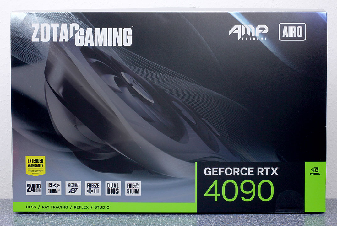
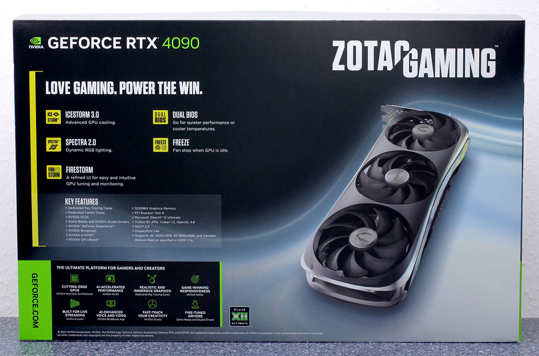
Packaging
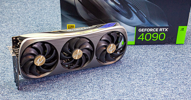
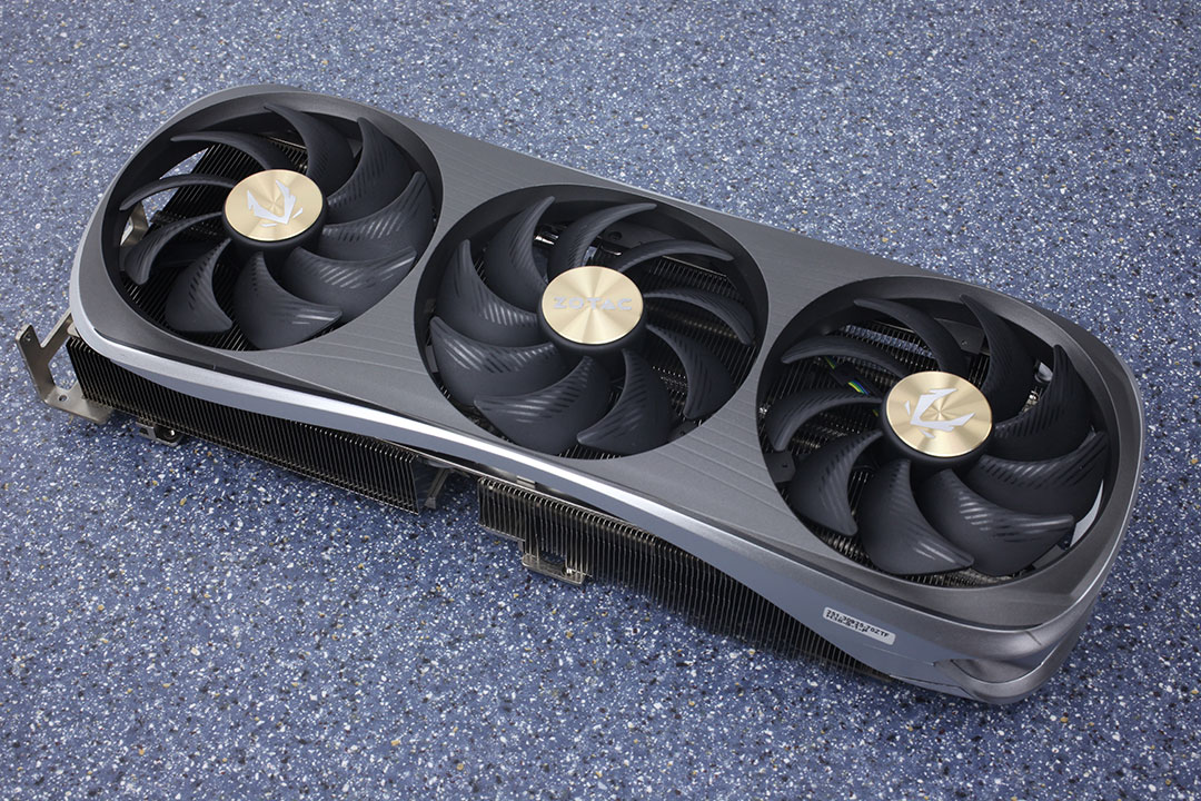
The Card
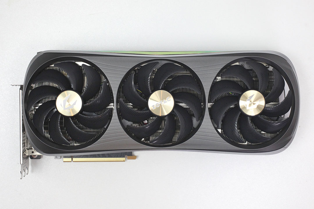

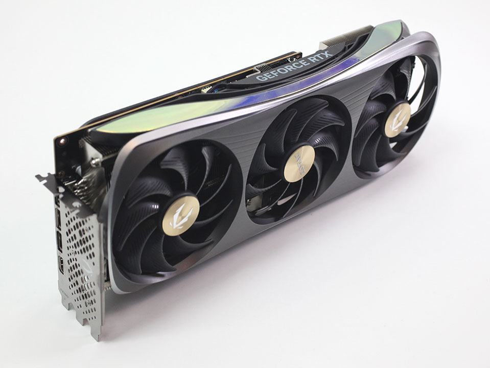
While most other GeForce RTX 40 cards are focusing on edgy designs with sharp corners, Zotac is taking an all-smooth approach. The curves on their card are almost female-elegant. On the back you get a high-quality metal backplate, the front cooler shroud is made from plastic.
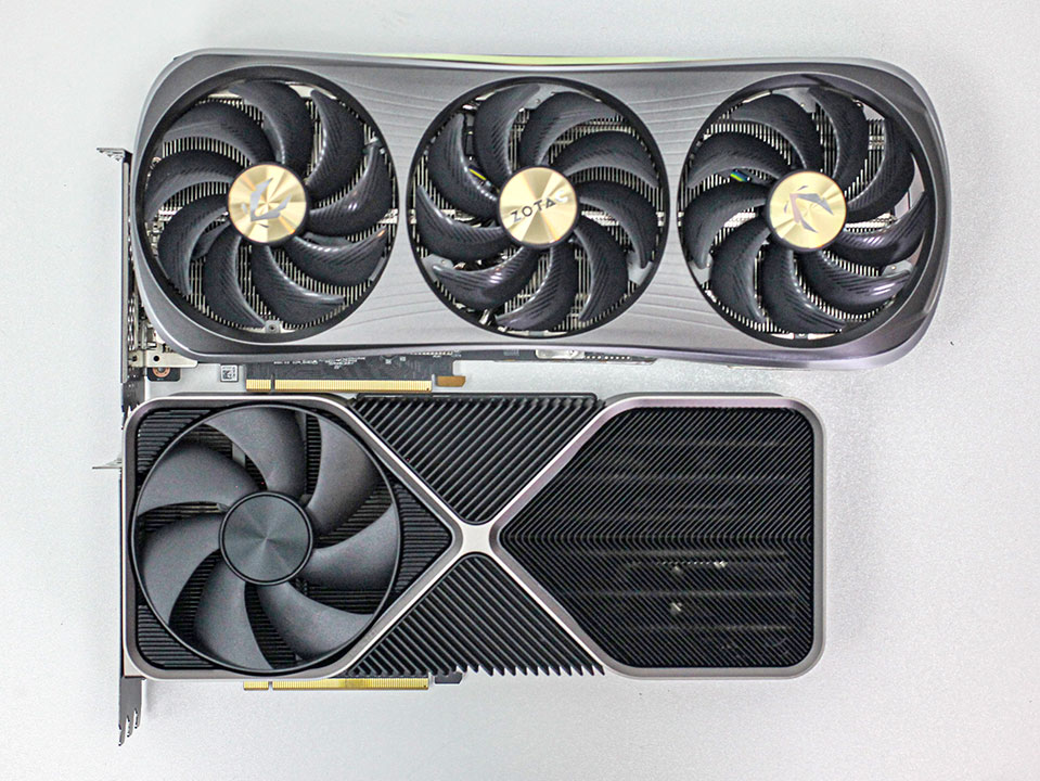

Even compared with the Founders Edition, which is already pretty big, the Zotac card is even larger.


Dimensions of the card are 36.0 x 15.0 cm, and it weighs 2044 g.


Installation requires four slots in your system.

Display connectivity includes three standard DisplayPort 1.4a ports and one HDMI 2.1a (same as Ampere).
NVIDIA introduced the concept of dual NVDEC and NVENC Codecs with the Ada architecture. This means there are two independent sets of hardware-accelerators; so you can encode and decode two streams of video in parallel or one stream at double the FPS rate. The new 8th Gen NVENC now accelerates AV1 encoding, besides HEVC. You also get an "optical flow accelerator" unit that is able to calculate intermediate frames for videos, to smooth playback. The same hardware unit is used for frame generation in DLSS 3.


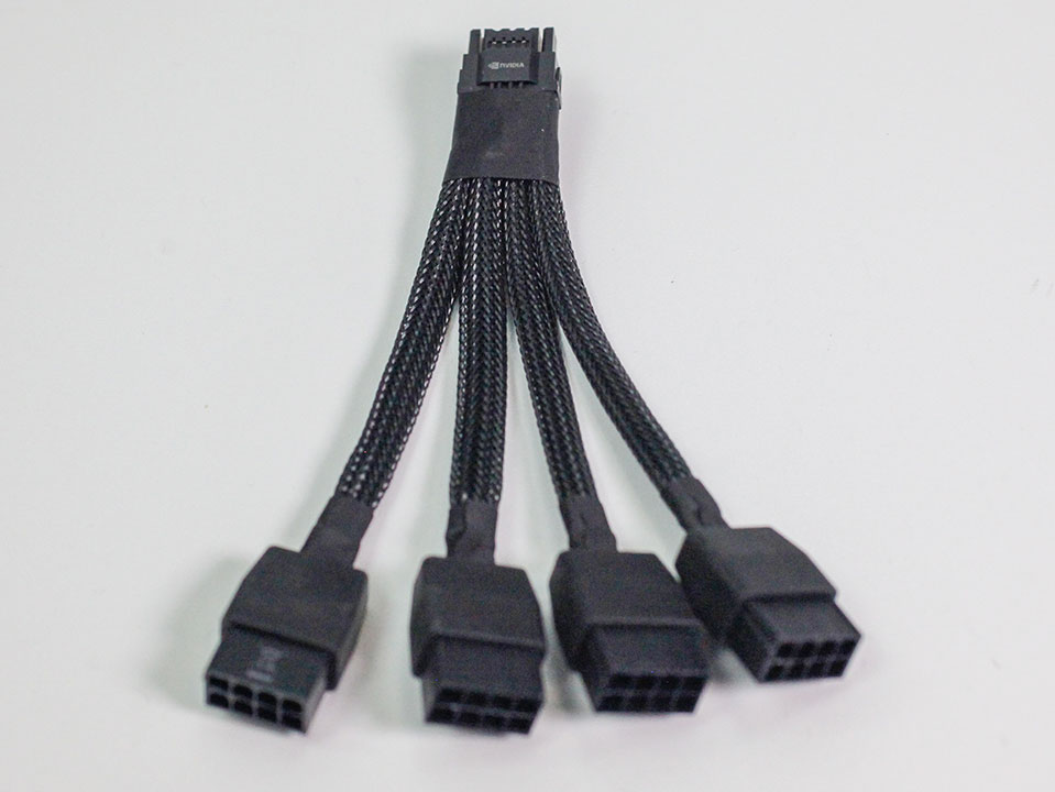
Just like the Founder Edition, the card uses the new 12+4 pin ATX 12VHPWR connector, which is rated for up to 600 W of power draw. An adapter cable from 4x PCIe 8-pin is included, you can also run the card with just three 8-pins.
Right next to the power connector you find the dual BIOS switch which lets you toggle between the default performance BIOS and a secondary quiet BIOS. Interestingly, Zotac chose to use a push button instead of a physical switch, which means you can only switch between the two when the card is powered up. Only power is sufficient, no need to go into BIOS or Windows, there's no need to install any software. After pressing the button, the RGB lights will flash red for performance BIOS and blue for quiet BIOS. The setting is saved between reboots and power offs, so no complaints from me.
Teardown
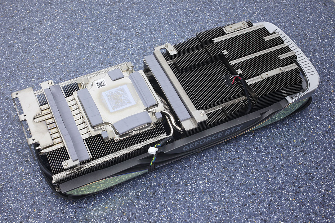
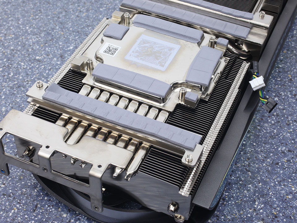
Zotac's thermal solution is huge and combines a vapor-chamber baseplate with nine heatpipes. The main heatsink also provides cooling for the memory chips and VRM circuitry.
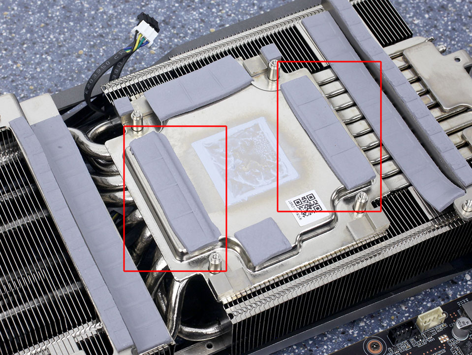
I noticed that the cooler doesn't make ideal contact with the memory chips on two sides. It seems that the vapor-chamber base is a little bit too small to cover the memory chips completely. The fact that the thermal pads were positioned slightly away from the edge didn't help either. With 76°C (82°C in quiet mode) memory temperatures are still perfectly fine, even though they are 4-6°C higher than on other RTX 4090 cards. Still MUCH better than the 100+°C that we saw on some GeForce 30 cards.
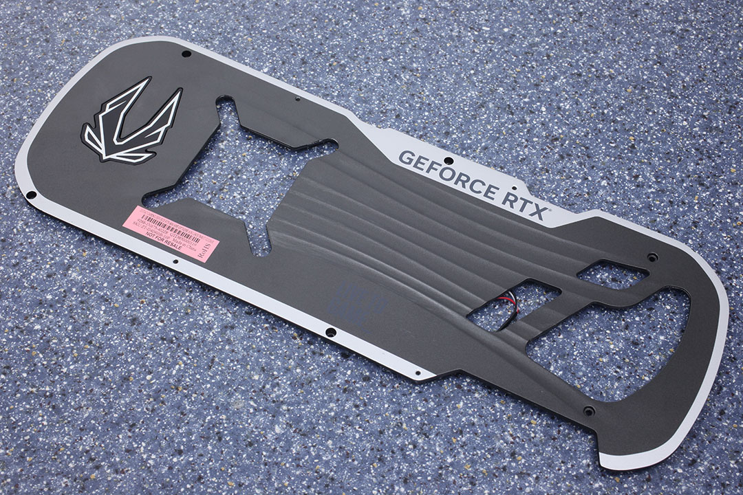
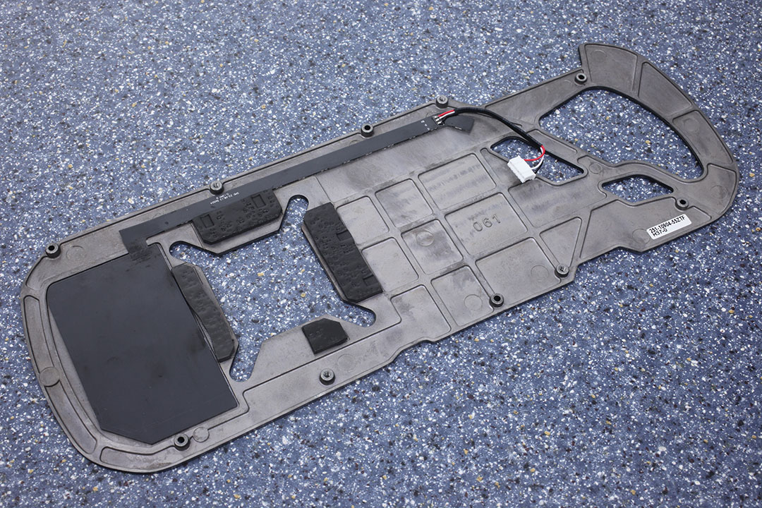
The backplate is made of metal and protects the card against damage during installation and handling, while also providing some structural integrity.
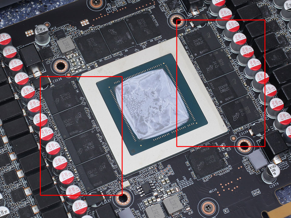
High-resolution PCB Pictures
These pictures are for the convenience of volt modders and people who would like to see all the finer details on the PCB. Feel free to link back to us and use these in your articles, videos or forum posts.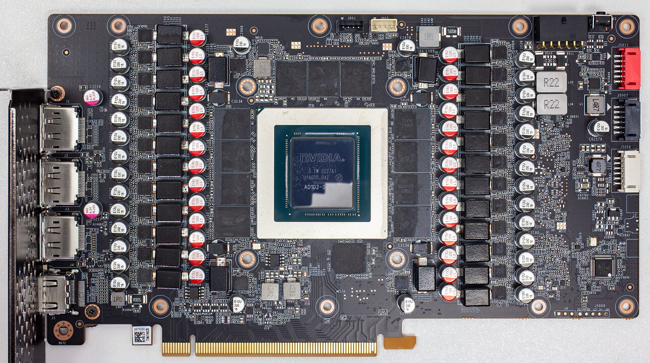
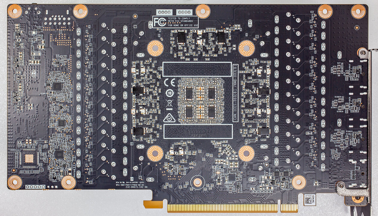
High-resolution versions are also available (front, back).
Our Patreon Silver Supporters can read articles in single-page format.
May 9th, 2024 14:09 EDT
change timezone
Latest GPU Drivers
New Forum Posts
- AM5 boot times improve RADICALLY with memory context restore enabled (3)
- Only some humans can see refresh rates faster than others, I am one of those humans. (235)
- Your way of cooling your PC? (89)
- TPU's Nostalgic Hardware Club (18504)
- Battery swap for cyberpower UPS (66)
- Last game you purchased? (275)
- Current Sales, Bundles, Giveaways (10231)
- What's a good option for a digital touchless thermometer? (17)
- Epic Games launcher's ridiculous CPU usage (33)
- Microsoft butchering Xbox Studios (26)
Popular Reviews
- CHERRY XTRFY M64 Pro Review
- Corsair iCUE Link RX120 RGB 120 mm Fan Review
- Bykski CPU-XPR-C-I CPU Water Block Review - Amazing Value!
- Finalmouse UltralightX Review
- Upcoming Hardware Launches 2023 (Updated Feb 2024)
- Corsair MP700 Pro SE 4 TB Review
- AMD Ryzen 7 7800X3D Review - The Best Gaming CPU
- Cougar Hotrod Royal Gaming Chair Review
- ASUS Radeon RX 7900 GRE TUF OC Review
- Meze Audio LIRIC 2nd Generation Closed-Back Headphones Review
Controversial News Posts
- Intel Statement on Stability Issues: "Motherboard Makers to Blame" (262)
- AMD to Redesign Ray Tracing Hardware on RDNA 4 (206)
- Windows 11 Now Officially Adware as Microsoft Embeds Ads in the Start Menu (167)
- NVIDIA to Only Launch the Flagship GeForce RTX 5090 in 2024, Rest of the Series in 2025 (144)
- Sony PlayStation 5 Pro Specifications Confirmed, Console Arrives Before Holidays (119)
- AMD's RDNA 4 GPUs Could Stick with 18 Gbps GDDR6 Memory (114)
- NVIDIA Points Intel Raptor Lake CPU Users to Get Help from Intel Amid System Instability Issues (106)
- AMD Ryzen 9 7900X3D Now at a Mouth-watering $329 (104)