 348
348
AMD Radeon R9 Fury X 4 GB Review
Test Setup »A Closer Look

AMD's cooling solution is a little technology marvel. It is made by Cooler Master and integrates waterblock, pump, and VRM cooling circuitry in one piece.

The next piece that goes off is the metal backplate, which helps protect the card against damage during handling, while adding to the product's visuals.
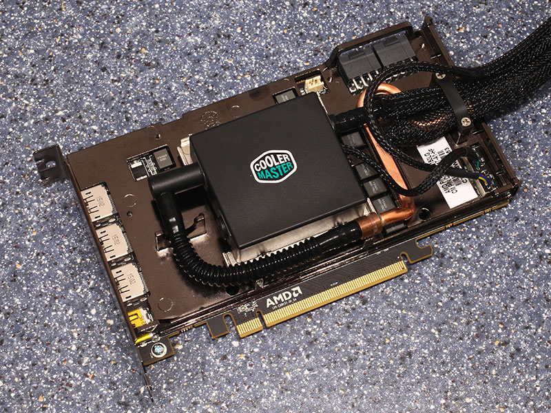
After removing the Radeon shroud (which is lit, by the way), we get to take a closer look at the watercooling components.

Note the piece of copper tubing that runs along the right side of the GPU. It cools the voltage regulation circuitry below it, an elegant solution. Other designs use a fan for that, which would add extra noise.


With the waterblock removed, we can finally get a first glimpse of the GPU, which is still covered by A LOT of thermal paste. The waterblock uses a copper baseplate with a milled-out section for the GPU; there is no additional milling for the HBM chips.


The radiator is your typical 120 mm variant, with a very quiet fan made by Nidec.

A row of LEDs will indicate the GPU's power draw, acting as the GPU's activity indicator. The left-most LED is green and will light up when the card is running in ZeroCore power mode (the pump and fan will not turn off in ZeroCore). You may change the color using the DIP switches to the left.
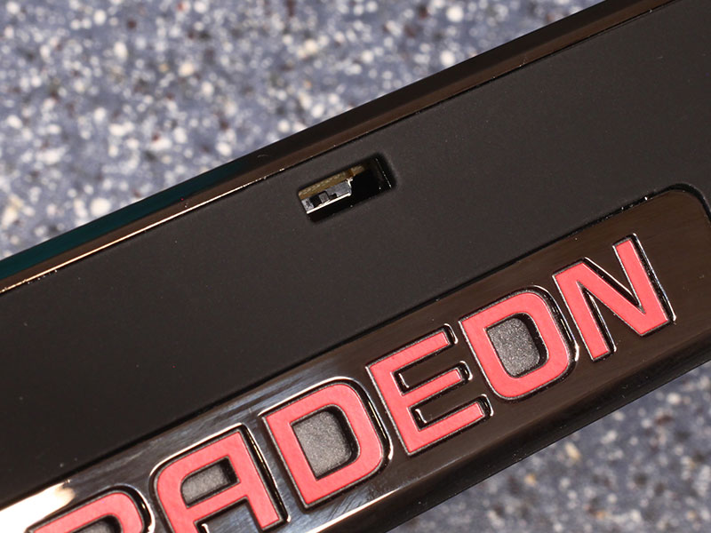
Like on most recent AMD Radeon products, a dual-BIOS switch is included, which serves as a fail-safe in case a BIOS flash goes wrong. The two BIOSes are identical.

Power delivery requires two 8-pin PCI-Express power connectors. This configuration is specified for up to 375 W power draw.

We've seen the IR 3567 voltage controller on the R9 390x/290X before. It supports software voltage control and monitoring via I2C and is well supported in overclocking software.

The HBM memory chips are by Hynix. They are specified to run at 500 MHz. The two stacks pictured in the photo are each comprised of five stacked silicon dies, four DRAM and one controller. A total of four stacks are installed, sitting on the silicon interposer (the colorful parts), together with the large GPU die.

AMD's Fiji graphics processor uses the GCN shader architecture. It is produced on a 28 nm process at TSMC, Taiwan, with 8.9 billion transistors on a 596 mm² die.
Apr 27th, 2024 20:35 EDT
change timezone
Latest GPU Drivers
New Forum Posts
- Ryzen Owners Zen Garden (7256)
- Usb 3.2 and usbc speeds became very slow (7)
- On ACER V3-772G GDDR5 laptop no display (5)
- Anyone know if Rufus gets around the SSE4.2 issue with Windows 11 24H2? (28)
- RTX 3080 and RX 6800XT video/graphics cards (4)
- Your PC ATM (34514)
- Best SSD for system drive (107)
- Core PL1 + GPU PL1 + Ring EDP OTHER (11)
- Which air cooler for a ryzen 9 5900x (168)
- Black screens leading to restarts (Event ID 18) on AMD platform since changing graphics card (45)
Popular Reviews
- Ugreen NASync DXP4800 Plus Review
- HYTE THICC Q60 240 mm AIO Review
- Palit GeForce RTX 4090 GameRock OC Review
- MSI GeForce RTX 4090 Suprim X Review
- Zotac GeForce RTX 4090 Amp Extreme Airo Review
- MOONDROP x Crinacle DUSK In-Ear Monitors Review - The Last 5%
- Thermalright Phantom Spirit 120 EVO Review
- ASUS GeForce RTX 4090 Matrix Platinum Review - The RTX 4090 Ti
- Colorful GeForce RTX 4090 Vulcan OC-V Review
- Upcoming Hardware Launches 2023 (Updated Feb 2024)
Controversial News Posts
- Windows 11 Now Officially Adware as Microsoft Embeds Ads in the Start Menu (139)
- Sony PlayStation 5 Pro Specifications Confirmed, Console Arrives Before Holidays (117)
- NVIDIA Points Intel Raptor Lake CPU Users to Get Help from Intel Amid System Instability Issues (106)
- AMD "Strix Halo" Zen 5 Mobile Processor Pictured: Chiplet-based, Uses 256-bit LPDDR5X (103)
- US Government Wants Nuclear Plants to Offload AI Data Center Expansion (98)
- AMD's RDNA 4 GPUs Could Stick with 18 Gbps GDDR6 Memory (95)
- Developers of Outpost Infinity Siege Recommend Underclocking i9-13900K and i9-14900K for Stability on Machines with RTX 4090 (85)
- Windows 10 Security Updates to Cost $61 After 2025, $427 by 2028 (84)