 41
41
ASUS GTX 1080 Strix Gaming 8 GB Review
Test Setup »A Closer Look

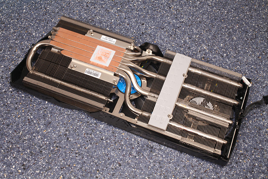
ASUS's thermal solution uses five heatpipes; four of these directly touch the GPU surface. You can also see a grey thermal pad that cools the voltage regulation circuitry.
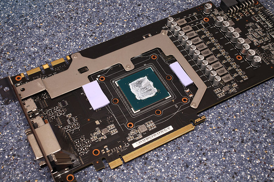
Once the main cooler is removed, a shiny metal bar becomes visible; it provides cooling for the memory chips.
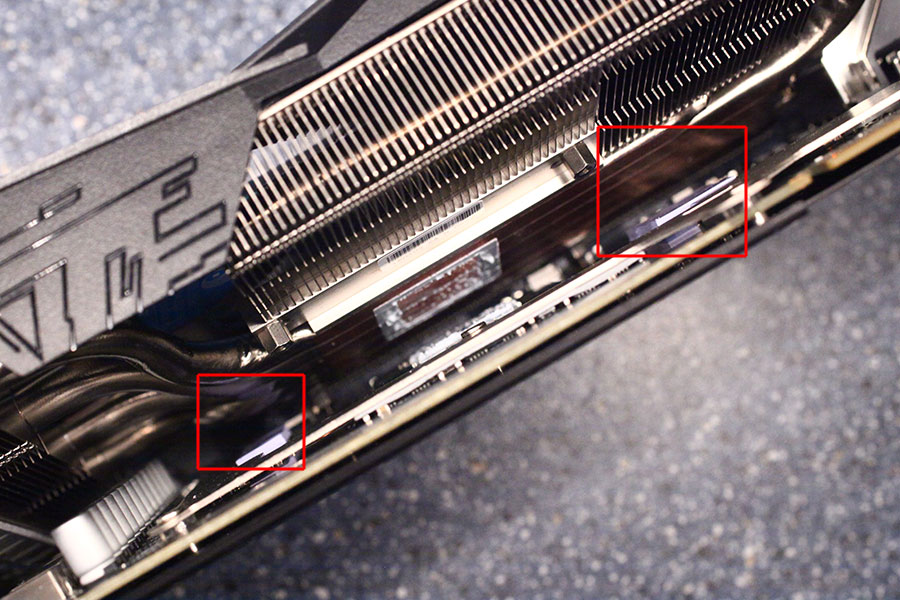
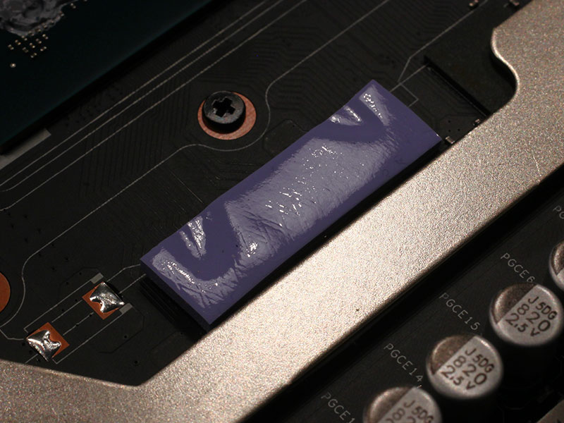
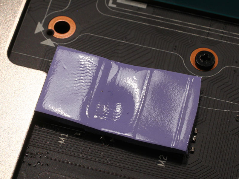
"Hold on, not so fast" I hear you say, what about those two orphaned thermal pads in the photos above? Well, they provide cooling for the memory chips not covered by the metal bar. I took some closeups and they make contact with the heatpipes. Even though it's not a lot, going by the indentations in the pads, it should be enough - the GDDR5X chips don't produce much heat anyway.
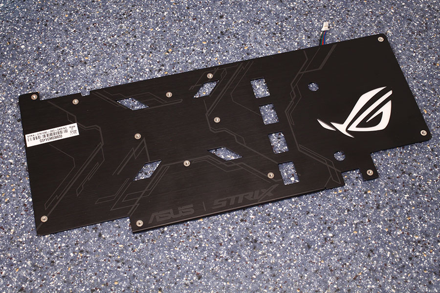
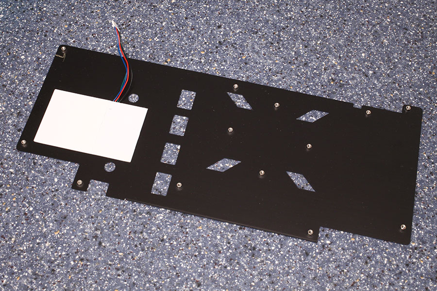
The backplate is made out of metal and has an RGB LED module that illuminates the ROG logo.
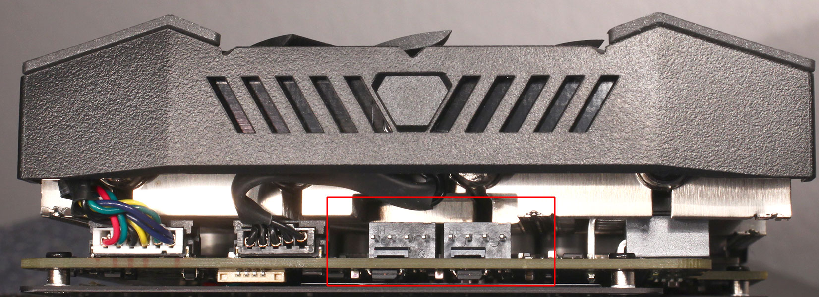
Near the back of the card are two fan connectors that are in sync with the GPU's fans. You could hook up two case fans that will stop completely outside of games. The main source of heat nowadays being the graphics card, attached case fans will run at the same speed as the GPU's fans that base their speed on how hot the card runs. A great idea!
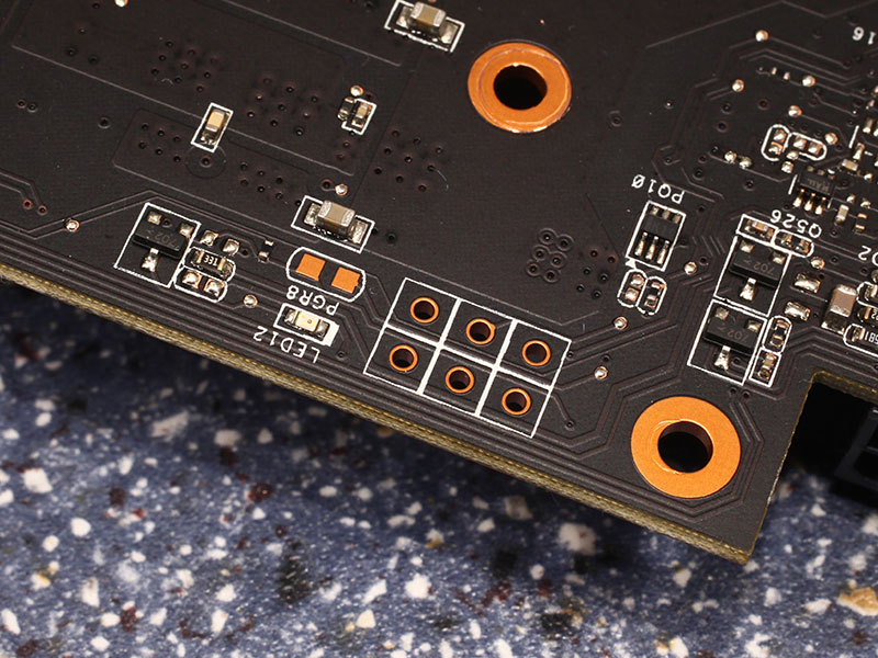
ASUS has also included what look to be solder OC tweaking points. They are not marked, so it'll be up to the overclockers to figure out what they do.
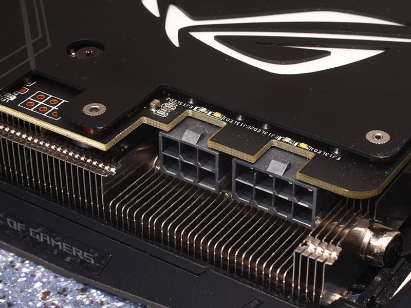
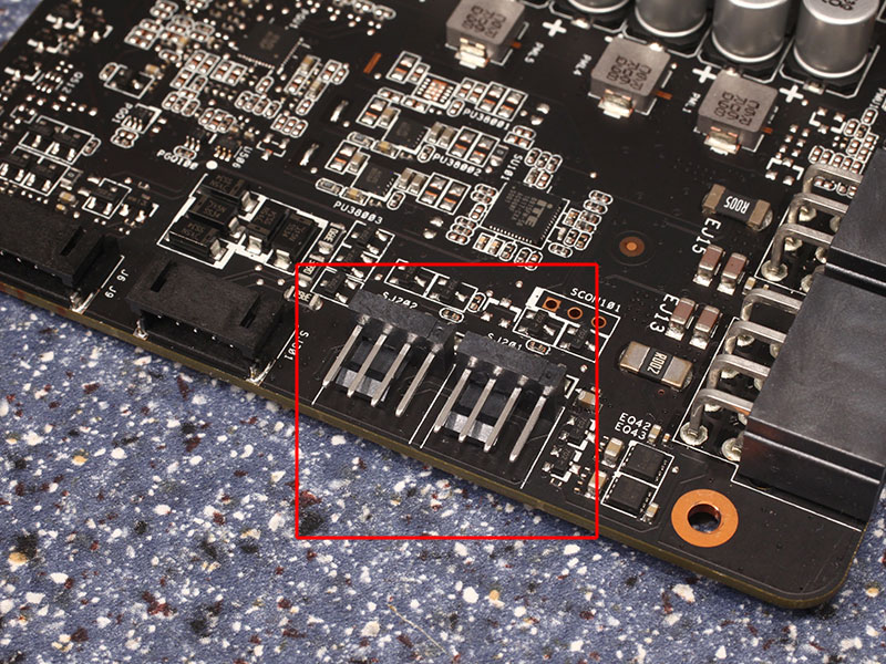
ASUS has upgraded the power input of their GTX 1080 to an 8-pin and a 6-pin. This input configuration is specified for up to 300 watts of power draw.
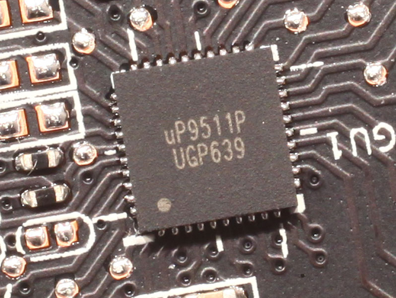
NVIDIA's Pascal is introducing a new voltage controller by uPI, the uP 9511P. Its exact feature set is currently unknown.

The GDDR5X memory chips are made by Micron and are marked with "D9TXS," which decodes to MT58K256M32JA-100. They are specified to run at 1250 MHz (10,000 MHz GDDR5X effective).

NVIDIA's GP104 graphics processor is the first consumer chip using the Pascal architecture. It is produced on a 16 nm process at TSMC, Taiwan, with a transistor count of 7.1 billion and a die size of 314 mm².
May 12th, 2024 04:14 EDT
change timezone
Latest GPU Drivers
New Forum Posts
- Purchased an AX1200i PSU as part of some forward planning, what tier is this PSU? (4)
- PSU Option for my PC (6)
- What's your latest tech purchase? (20516)
- monitor w good contrast and viewing angle for my sister with eye problems (14)
- Flash VBIOS to turn RX 580 2048SP into RX 570 (38)
- X670 owners, what kind of PCH temps do you you see? (20)
- What's an inexpensive AIO product line with a strong pump and low price? (102)
- Homeworld 3 [Official Thread] (13)
- The Filthy, Rotten, Nasty, Helpdesk-Nightmare picture clubhouse (2629)
- 2024 and STILL no dark mode? (33)
Popular Reviews
- ZMF Caldera Closed Planar Magnetic Headphones Review
- ThundeRobot ML903 NearLink Review
- Corsair MP700 Pro SE 4 TB Review
- Bykski CPU-XPR-C-I CPU Water Block Review - Amazing Value!
- CHERRY XTRFY M64 Pro Review
- Upcoming Hardware Launches 2023 (Updated Feb 2024)
- ASRock NUC BOX-155H (Intel Core Ultra 7 155H) Review
- Corsair iCUE Link RX120 RGB 120 mm Fan Review
- AMD Ryzen 7 7800X3D Review - The Best Gaming CPU
- ASUS Radeon RX 7900 GRE TUF OC Review
Controversial News Posts
- Intel Statement on Stability Issues: "Motherboard Makers to Blame" (266)
- AMD to Redesign Ray Tracing Hardware on RDNA 4 (206)
- Windows 11 Now Officially Adware as Microsoft Embeds Ads in the Start Menu (171)
- NVIDIA to Only Launch the Flagship GeForce RTX 5090 in 2024, Rest of the Series in 2025 (147)
- Sony PlayStation 5 Pro Specifications Confirmed, Console Arrives Before Holidays (119)
- AMD's RDNA 4 GPUs Could Stick with 18 Gbps GDDR6 Memory (114)
- NVIDIA Points Intel Raptor Lake CPU Users to Get Help from Intel Amid System Instability Issues (106)
- AMD Ryzen 9 7900X3D Now at a Mouth-watering $329 (104)