 68
68
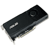
ASUS GeForce GTX 470 Fermi Review
Test Setup »A Closer Look

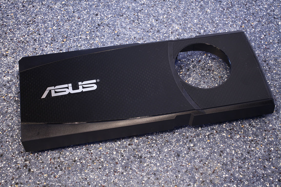

The first step in disassembly is removing the black plastic fan shroud. It is a simple piece of plastic that protects the heatsink and creates an air channel for the fan's air to move out of the card.


You will find five heatpipes on the main heatsink that use DirectTouch technology to make optimum contact with the GPU core. Heat is then transferred to a large number of fins where it is dissipated.

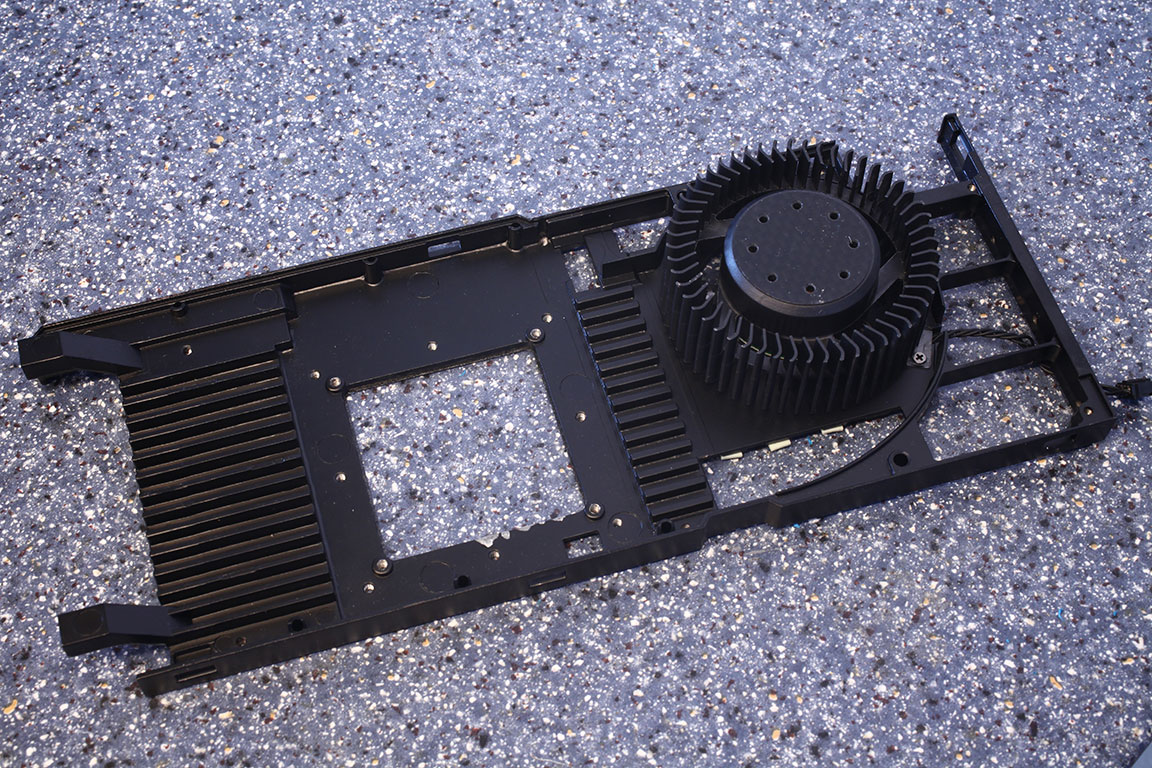

The last piece that goes off is a big black metal heatsink that covers all the "minor" components of the graphics card, like memory and voltage regulation circuitry. This approach makes it easy for water cooling and extreme cooling to be attached to the GPU only without having to worry about cooling the rest of the components.
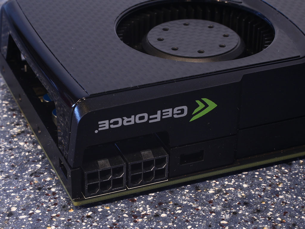
Dual six-pin power connectors are already a first hint that the power consumption of the GeForce GTX 470 isn't going to be as epic as that of the GTX 480.

The GDDR5 memory chips are made by Samsung, and carry the model number K4G10325FE-HC05. They are specified to run at 2000 MHz (4000 MHz GDDR5 effective).

OnSemi's NCP5388 is a reasonable priced voltage regulator, unfortunately it does not have I2C voltage control.
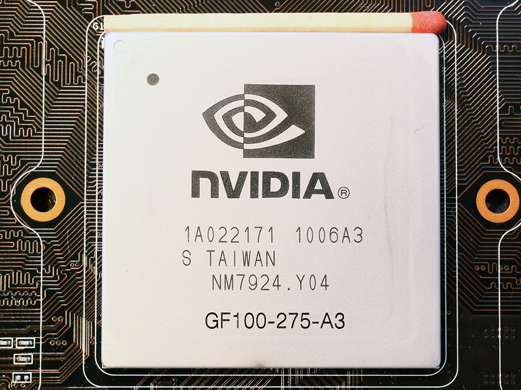
NVIDIA's GeForce 100 graphics processor is made on a 40 nm process at TSMC Taiwan. It uses approximately 3.2 billion transistors which makes it the most complex GPU built to-date. Please note that the silvery metal surface you see is the heatspreader of the GPU which measures 42.3 x 42.3 mm. The actual GPU die is sitting under the heatspreader, its dimensions are not known. NVIDIA did not communicate a die size measurement to the press.
Apr 26th, 2024 12:37 EDT
change timezone
Latest GPU Drivers
New Forum Posts
- 2022-X58/1366 PIN Motherboards NVME M.2 SSD BIOS MOD Collection (657)
- DTS DCH Driver for Realtek HDA [DTS:X APO4 + DTS Interactive] (1909)
- checkup (1)
- Help me to OC my 5700X (10)
- XFX RX470 8GB no video and error 43 (28)
- The TPU UK Clubhouse (24788)
- Secure boot already open help (9)
- im new to throttelstop and i think i messed it up by copying others any hints would be very much aprreciated (4)
- Cs2 Freezing in Rx 580 (5)
- Ghost of Tsushima PC Port !!!! (15)
Popular Reviews
- HYTE THICC Q60 240 mm AIO Review
- MOONDROP x Crinacle DUSK In-Ear Monitors Review - The Last 5%
- Alienware Pro Wireless Gaming Keyboard Review
- Upcoming Hardware Launches 2023 (Updated Feb 2024)
- Thermalright Phantom Spirit 120 EVO Review
- FiiO K19 Desktop DAC/Headphone Amplifier Review
- ASUS Radeon RX 7900 GRE TUF OC Review
- RTX 4090 & 53 Games: Ryzen 7 5800X vs Ryzen 7 5800X3D Review
- NVIDIA RTX 4090: 450 W vs 600 W 12VHPWR - Is there any notable performance difference?
- Sapphire Radeon RX 7900 GRE Pulse Review
Controversial News Posts
- Windows 11 Now Officially Adware as Microsoft Embeds Ads in the Start Menu (127)
- Sony PlayStation 5 Pro Specifications Confirmed, Console Arrives Before Holidays (117)
- NVIDIA Points Intel Raptor Lake CPU Users to Get Help from Intel Amid System Instability Issues (106)
- AMD "Strix Halo" Zen 5 Mobile Processor Pictured: Chiplet-based, Uses 256-bit LPDDR5X (102)
- US Government Wants Nuclear Plants to Offload AI Data Center Expansion (98)
- AMD's RDNA 4 GPUs Could Stick with 18 Gbps GDDR6 Memory (92)
- Developers of Outpost Infinity Siege Recommend Underclocking i9-13900K and i9-14900K for Stability on Machines with RTX 4090 (85)
- Windows 10 Security Updates to Cost $61 After 2025, $427 by 2028 (84)