 82
82
ASUS M5A97 EVO AM3+ Review
BIOS Walkthrough »The Board - A Closer Look

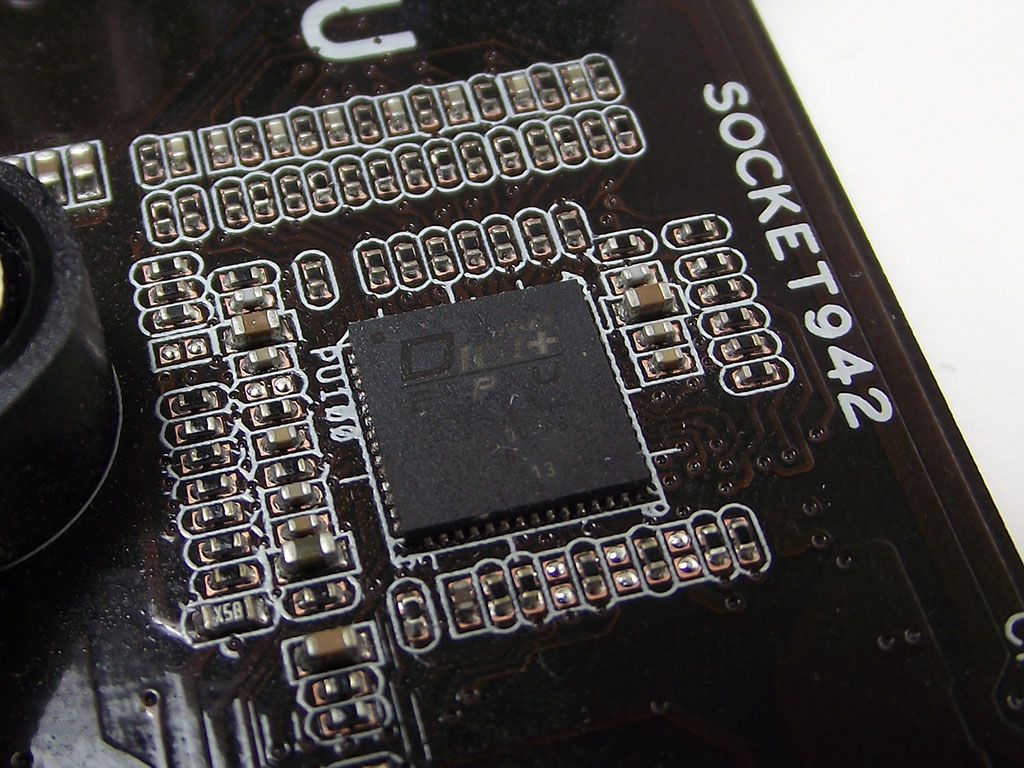

Our usual first item to look at, of course, is the BIOS chip itself, which in this instance, is supplied by Winbond. Nestled securely in a socket that makes user replacement fairly simple, the M5A97 EVO shows that user experience is first and foremost with ASUS. Once the BIOS has booted the M5A97 EVO up, the real brains of the board, the EPU and TPU chips, are in full operation. We've covered these specific parts in our P8P67 PRO review before, and the exact same parts are here on the M5A97 EVO. The second picture shows the EPU/DIGI+ chip, and the incomplete printing of the label should give you an idea of just how many products feature these ASUS-exclusive parts. Offering full customization of the board's VRM, from current capabilities, to even the frequency the VRM operates at, is something we were surprised to see here, yet because our testing has proven that this solution is one of the best out there, it was most definitely a pleasant surprise.


There are several switches placed around the board; the EPU and MemOK! switches are aptly located to the right of the DIMM slots, and the TPU switch is found hiding right below the SATA ports on the board's right edge. The MemOK! switch, when depressed, will start a boot-up routine that will test the installed memory, and then boot the board with stable voltages and timings, allowing users not only to get into the BIOS to revert from bad settings, but also allowing users to save the settings suggested by the MemOK function. the EPU switch offers automatic power profile adjustments focused on lowering overall board power consumption, while the TPU does the exact opposite, providing an easy way for users to overclock their system, with settings that have been extensively tested to provide full stability with the majority of CPU and memory on the market today. As always though, there is no guarantee that the settings will be 100% stable, so if you do happen to use this feature, be sure to properly test for stability after flipping the TPU switch.


The M5A97 EVO's VRM is controlled directly by the EPU/DIGI+ chip, unlike the Intel boards we looked at previously. Close examination of the VRM components shows a traditional hi/low MOSFET configuration, with input drivers located next to each MOSFET pair. The dual DIMM phases feature a similar config, with the input driver located next to the MemOK switch. The northbridge VRM is similar as well, employing three MOSFETs like the CPU phases, rather than the two seen in the DIMM VRM. All three VRM sections are controlled by both the TPU and EPU chips, which together creates the "Dual Intelligent Processor" technology mentioned on the box front.
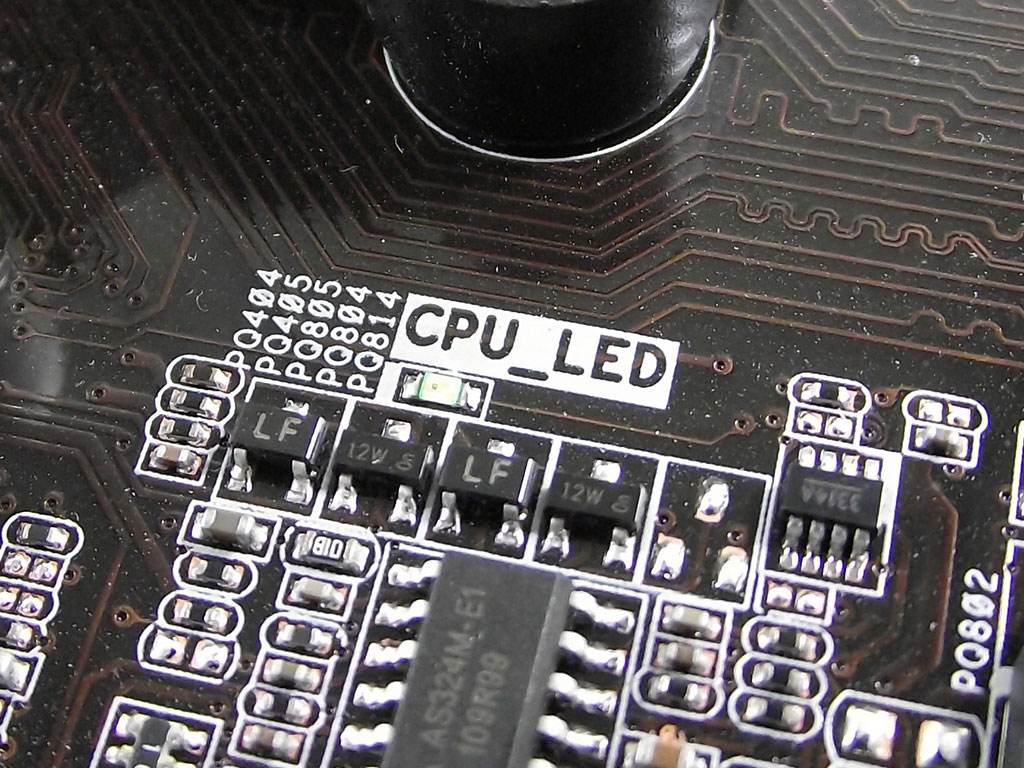

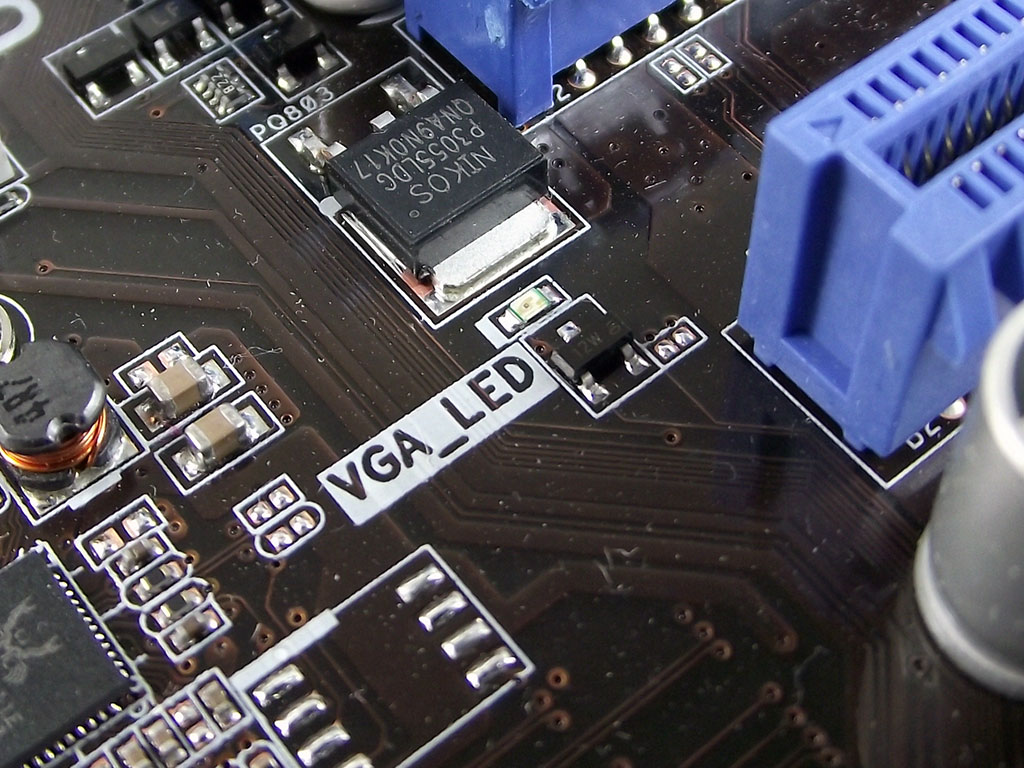

Once the board's been powered on, there is a series of four LEDs that light up in succession as the board boots, functioning as a POST code reader, of sorts. Should the boot process fail during any of the steps, the LED will remain lit, giving the user a clear indicator as to what part is causing the boot failure, a very useful tool when troubleshooting overclocks.
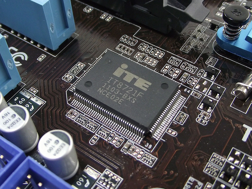

For Super I/O functionality, we find an ITE IT8721F, a part used quite often on other products. As is usual, this chip is responsible for fan control and monitoring. The VIA VT6308P drives the FireWire ports found on the backplane, as well as the internal FireWire port header found near the board's edge.


The included Realtek ALC892 HD codec supports 7.1+2 audio, and meets Microsoft's WLP3.x audio requirements. Using DACs that output a 97 db SNR, and ADCs with a 90 db SNR, it supports 44.1k/48k/96k/192 kHz sampling at 16-, 20- and 24-bit, including full support for HD audio formats featuring Content Protection, providing supporting software is used. It is also DirectSound 3D compatible, so no area of usage or functionality is overlooked. ASUS has also sourced the LAN controller for the ASUS M5A97-EVO from Realtek; a utterly common RTL8111E PCIe part, located near the board's left edge just under the rear I/O assembly.
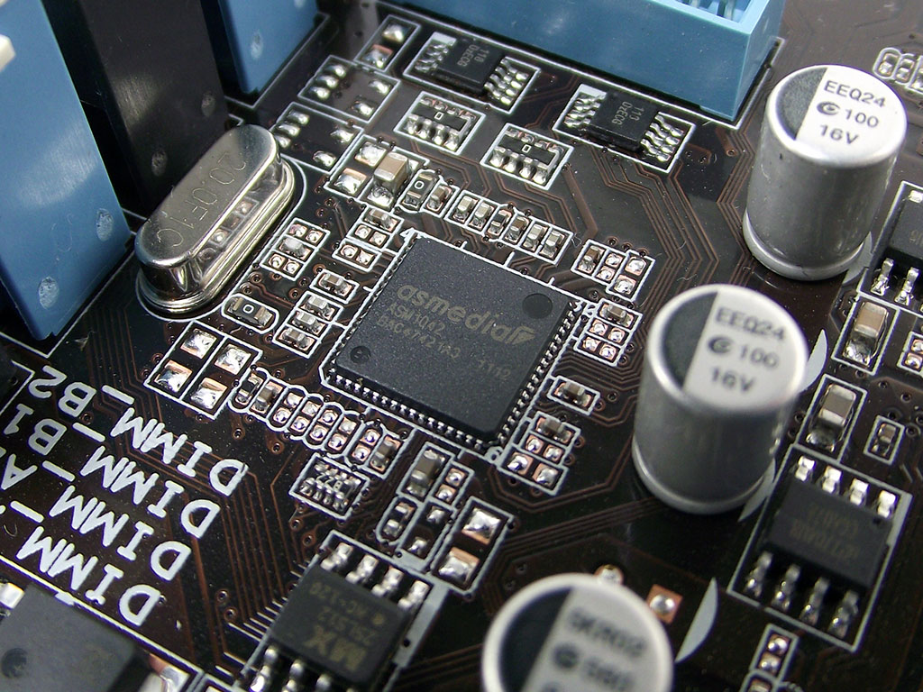


For USB 3.0 support, we find two matching Asmedia AS1042 PCIe controllers, with one under the DIMM slots, supporting the internal port we find nearby the controller itself, while the second is hidden between the VRM heatsink, and the rear I/O assembly. While these controllers are not as familiar as the NEC/Renesas controller, which is far more common, we have found Asmedia controllers to be used on many recently-released ASUS products.


Situated between the PCIe x16 slots we find an ICS clock generator, none other than the ICS 9LPRS477DKL. Specifically designed for the AMD platform, it controls all host clocks, CPU and Southbridge included, and is accessed via an SMBUS interface. The final board component, from JMicron, the JMB362, provides support for the dual eSATA 3.0 Gb/s ports found on the rear I/O. Having been on the market for several years, the JMB362 seems to fit in perfectly with what we expect from the ASUS M5A97 EVO.
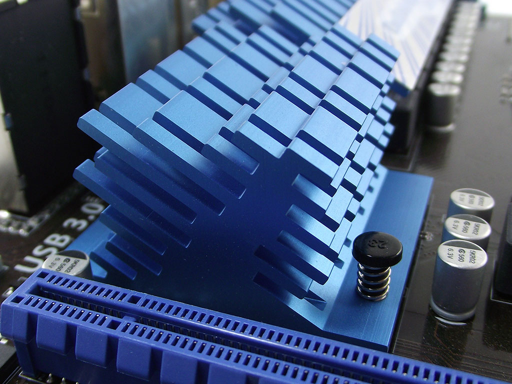

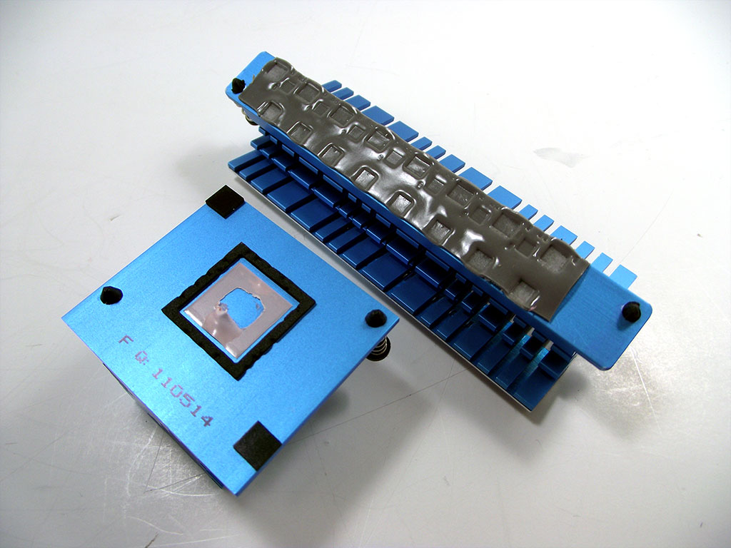
For cooling, ASUS has equipped the M5A97 EVO with several blue-anodized aluminum passive heatsinks, which you can see in the pictures above. The Northbridge heatsink is fairly beefy, and the same profile design is carried over to the VRM heatsink as well. the Southbridge heatsink, however, is quite small, providing several millimeters of clearance for installed expansion cards, yet through our testing, proved more than adequate. Upon removal of the VRM heatsink, we noticed near perfect contact from end to end, such that we do hope to see the same thermal interface pad used on other products. You can see clear impressions made by the VRM's components, ensuring that every critical component gets the cooling it needs, extremely vital when it comes to overclocking. The northbridge heatsink uses a gummy pink thermal interface material that pulled away from both the cooler and the northbridge itself when we removed the cooler. This material is such that we recommend that the northbridge cooling is NOT removed under any circumstances, as it was quite difficult to clean off of the northbridge chipset. This also prompted us to not remove the southbridge heatsink; we only removed the northbridge cooler as it was necessary in order to remove the MOSFET cooler.


In the above pictures you can clearly see the excellent contact the pink thermal interface provided, as well as how the thinner-than-paper material pulled up from the chipset when we removed the cooler. After nearly half an hour of very careful cleaning, we managed to reveal the new AMD970 chipset, as you can see in the second picture above. The manufacture date listed tells us that we got the final board shortly after ASUS got the chipsets from AMD, as the chip was "minted" during the 18th week of 2011, coinciding with the middle of May.
We're not done yet though; hit the link next page link to take a look at one of our favorite features, the BIOS.
May 5th, 2024 11:05 EDT
change timezone
Latest GPU Drivers
New Forum Posts
- [HELP] AMD GPU FINDING BIOS PROBLEM (1)
- Need advice for UPS that will be use only for bios updates (14)
- RTX 6000 ADA Problem. (6)
- im new to throttelstop and i think i messed it up by copying others any hints would be very much aprreciated (7)
- Resolution problems in-game with Av receiver (windows 11) (3)
- Should I install Windows 10 or 11 for my new device (68)
- Battery swap for cyberpower UPS (54)
- Is updating BIOS to beta versions a good idea if you have the most recent version installed but still face issues? (9)
- Strange system crashes out of nowhere, help (26)
- What are you playing? (20572)
Popular Reviews
- Finalmouse UltralightX Review
- Meze Audio LIRIC 2nd Generation Closed-Back Headphones Review
- ASRock NUC BOX-155H (Intel Core Ultra 7 155H) Review
- Montech Sky Two GX Review
- Cougar Hotrod Royal Gaming Chair Review
- Upcoming Hardware Launches 2023 (Updated Feb 2024)
- Alienware Pro Wireless Gaming Keyboard Review
- AMD Ryzen 7 7800X3D Review - The Best Gaming CPU
- HYTE THICC Q60 240 mm AIO Review
- Logitech G Pro X Superlight 2 Review - Updated with 4000 Hz Tested
Controversial News Posts
- Intel Statement on Stability Issues: "Motherboard Makers to Blame" (240)
- Windows 11 Now Officially Adware as Microsoft Embeds Ads in the Start Menu (167)
- AMD to Redesign Ray Tracing Hardware on RDNA 4 (147)
- Sony PlayStation 5 Pro Specifications Confirmed, Console Arrives Before Holidays (117)
- AMD's RDNA 4 GPUs Could Stick with 18 Gbps GDDR6 Memory (114)
- NVIDIA Points Intel Raptor Lake CPU Users to Get Help from Intel Amid System Instability Issues (106)
- AMD Ryzen 9 7900X3D Now at a Mouth-watering $329 (104)
- AMD "Strix Halo" Zen 5 Mobile Processor Pictured: Chiplet-based, Uses 256-bit LPDDR5X (103)