 53
53
NVIDIA Turing GeForce RTX Technology & Architecture
GeForce RTX 2070, 2080 & 2080 Ti »Architecture
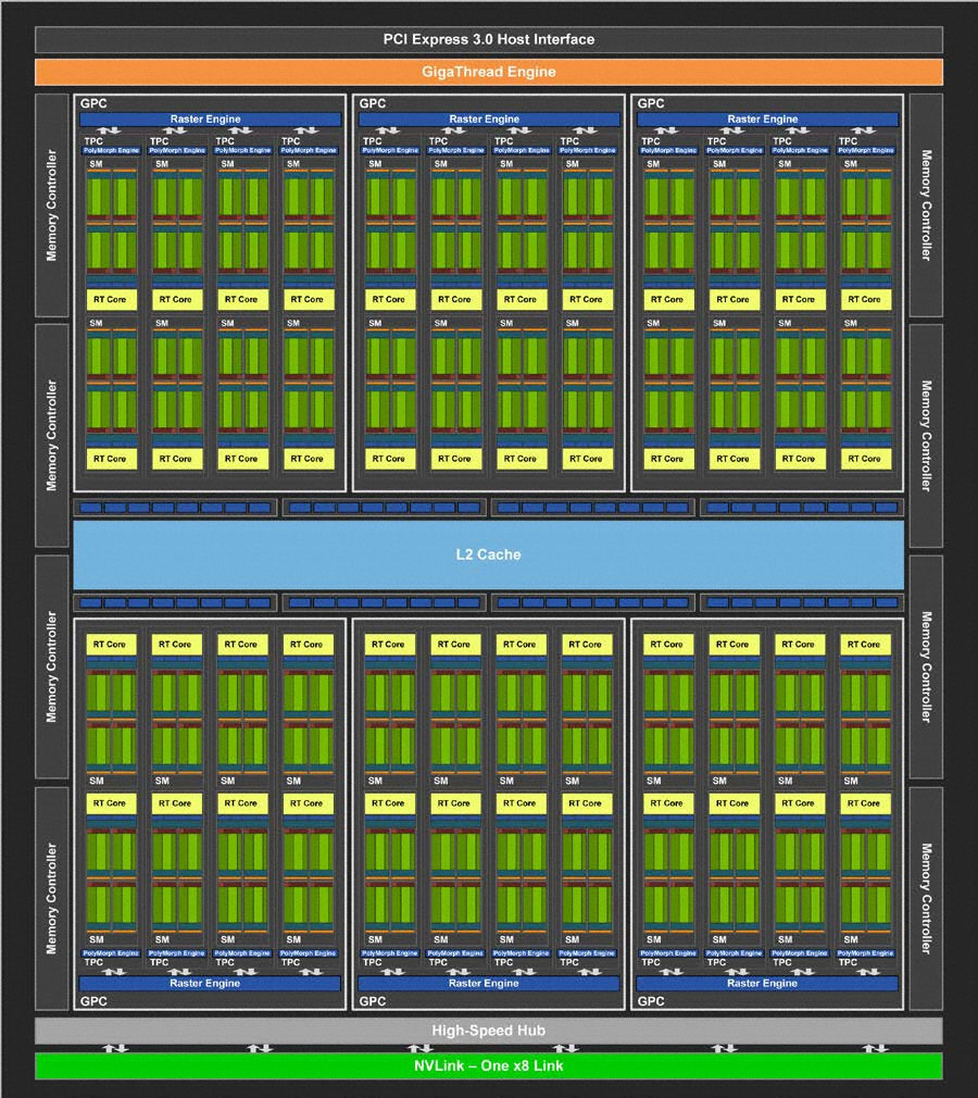
When NVIDIA released the first die-shot of Turing, it looked unlike any GPU die we'd seen from NVIDIA in a decade. Block-diagrams reveal that the first two Turing implementations, TU102 and TU104, more or less retain the component hierarchy of their predecessors needed to make a modern GPU work, but pack big changes to the SM (streaming multiprocessors), indivisible sub-units of the GPU, with the introduction of RT Cores and Tensor Cores, and a new Warp Scheduler that allows concurrent INT32 and FP32 execution, a feature that could improve the chip's overall asynchronous compute functions. We will dive deeper into the mechanics of a Turing CUDA core, SM, RT core, and Tensor cores, on subsequent pages.
Turing TU102
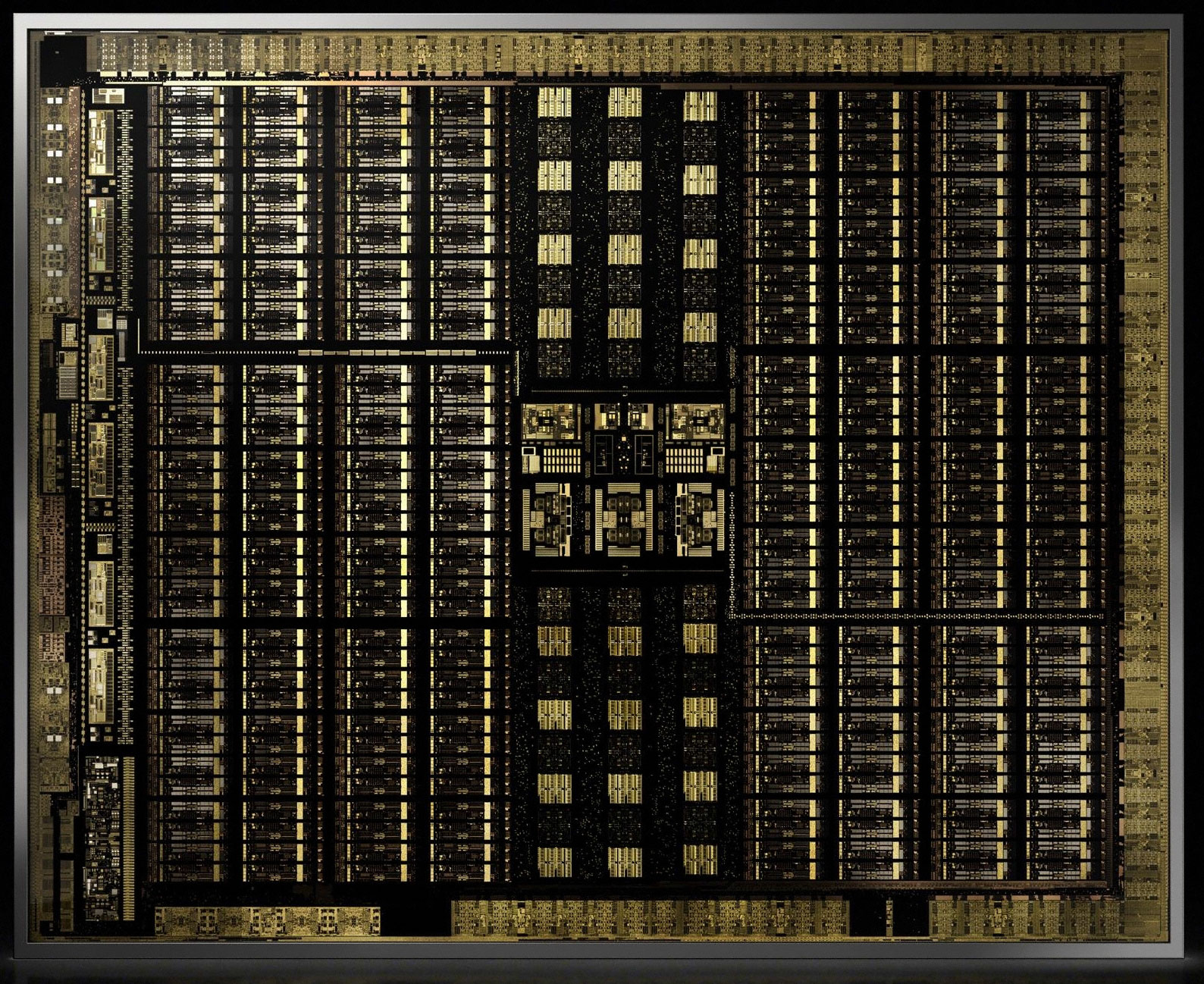
The Turing TU102 is the biggest single piece of non-storage silicon ever conceived. Built on the 12 nm silicon fabrication process like the rest of the Turing family, this chip packs a whopping 18 billion transistors and promises a TDP of just 250 W. The chip is armed with six GPCs (graphics processing clusters), which each pack twelve streaming multiprocessors (SM), the indivisible sub-unit of the GPU. There are hence 72 SMs across the TU102.
The addition of Tensor Cores and RT Cores leaves room for just 64 CUDA cores per SM, or 768 across a GPC, and 4,608 per die. Unlike the GV100, a Tensor Core takes up approximately eight times the die area of CUDA cores, and the SM has 8 Tensor Cores, or 96 Tensor Cores per GPC and 576 across the whole GPU. The RT core is the largest indivisible component in an SM, and there is only one of these per SM, 12 per GPC, and 72 across the die. A 384-bit GDDR6 memory bus handles up to 24 GB of GDDR6 memory.
Alas, the GeForce RTX 2080 Ti, like its predecessor, the GTX 1080 Ti, does not max out the TU102 silicon. Only 68 out of 72 SMs are enabled, which work out to 4,352 CUDA cores, 544 Tensor Cores, and 68 RT Cores. The memory bus, too, is narrowed down to 352-bit, driving 11 GB of memory. With Turing, NVIDIA put brakes on doubling memory amounts with each passing generation. Perhaps, the state of the DRAM industry is to blame here, and also the lack of a use case for twice the memory over the previous generation.
Turing TU104
The Turing TU104 will go down as the poster boy of the Turing architecture, much like its long line of predecessors, like the GK104 "Kepler" (GTX 680). This chip powers the GeForce RTX 2080, which interestingly, does not max out all components physically present on the chip. Perhaps the rumored RTX 2080+ could do just that.Another key dissimilarity the TU104 has over its predecessors is its GPC count in comparison to their bigger counterparts. The TU104 has the same exact number of GPCs as the TU102, at 6, with the only difference being SM count per GPC. While the TU102 has 12 SMs per GPC, the TU104 has 8. These SMs are of the same configuration as the TU102.
A maxed out TU104 would hence have 3,072 CUDA cores, 384 Tensor Cores, and 48 RT cores. The RTX 2080 does not max this chip out, and instead has two of its SMs disabled. This translates to 2,944 CUDA cores, 368 Tensor Cores, and 46 RT cores. Luckily, the memory interface is untouched. The 256-bit wide GDDR6 memory bus pulls 8 GB of memory on the RTX 2080.
Turing TU106
The TU106 is a very interesting chip, and NVIDIA is building the RTX 2070, not the RTX 2060 series, on this chip. Predecessors of the RTX 2070 (GTX 1070, GTX 970, etc.,) have traditionally been based on TU104's predecessors, with a few streaming multiprocessors being disabled. With the RTX 2070, NVIDIA decided to go with a physically smaller chip than the TU104, probably to minimize costs for this fast-moving, high-volume SKU.
The TU106 does not exactly succeed the GP106. It's half the chip the TU102 is. The chip has three GPCs, each of which has 12 SMs, just like the TU102 and unlike the TU104, which has 8 SMs per GPC. The 256-bit GDDR6 memory interface is carried over from the TU104.
In being a "half TU102," the TU106 hence has 36 SMs, or 768 CUDA cores per GPC. This works out to 2,304 CUDA cores in total. The Tensor Core count is 288, and 36 RT cores. The RTX 2070 maxes out this chip.
The TU106 does not feature the NVLink interface, and hence, the RTX 2070 lacks SLI support, which is quite unfortunate for a $500 graphics card.
Apr 25th, 2024 13:44 EDT
change timezone
Latest GPU Drivers
New Forum Posts
- What are you playing? (20527)
- Black screen after muting (0)
- How to check flatness of CPUs and coolers - INK and OPTICAL INTERFERENCE methods (111)
- Alphacool CORE 1 CPU block - bulging with danger of splitting? (11)
- Ghetto Mods (4321)
- Random blue screen from winload.efi error (0xc000000e) (2)
- Meta Horizon OS (20)
- WCG Daily Numbers (12497)
- Share your AIDA 64 cache and memory benchmark here (2917)
- Best SSD for system drive (76)
Popular Reviews
- Fractal Design Terra Review
- Thermalright Phantom Spirit 120 EVO Review
- Corsair 2000D Airflow Review
- Minisforum EliteMini UM780 XTX (AMD Ryzen 7 7840HS) Review
- ASUS GeForce RTX 4090 STRIX OC Review
- NVIDIA GeForce RTX 4090 Founders Edition Review - Impressive Performance
- ASUS GeForce RTX 4090 Matrix Platinum Review - The RTX 4090 Ti
- MSI GeForce RTX 4090 Suprim X Review
- MSI GeForce RTX 4090 Gaming X Trio Review
- Gigabyte GeForce RTX 4090 Gaming OC Review
Controversial News Posts
- Sony PlayStation 5 Pro Specifications Confirmed, Console Arrives Before Holidays (116)
- NVIDIA Points Intel Raptor Lake CPU Users to Get Help from Intel Amid System Instability Issues (106)
- AMD "Strix Halo" Zen 5 Mobile Processor Pictured: Chiplet-based, Uses 256-bit LPDDR5X (101)
- Windows 11 Now Officially Adware as Microsoft Embeds Ads in the Start Menu (98)
- US Government Wants Nuclear Plants to Offload AI Data Center Expansion (98)
- AMD's RDNA 4 GPUs Could Stick with 18 Gbps GDDR6 Memory (85)
- Developers of Outpost Infinity Siege Recommend Underclocking i9-13900K and i9-14900K for Stability on Machines with RTX 4090 (85)
- Windows 10 Security Updates to Cost $61 After 2025, $427 by 2028 (84)