 94
94
ZOTAC GeForce GTX 465 Review
Test Setup »A Closer Look


The first step in disassembly is removing the black plastic fan shroud. It is a simple piece of plastic that protects the heatsink and creates an air channel for the fan's air to move out of the card.


You will find five heatpipes on the main heatsink that use DirectTouch technology to make optimum contact with the GPU core. Heat is then transferred to a large number of fins where it is dissipated.
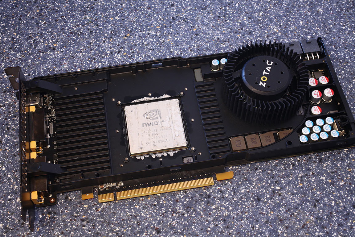

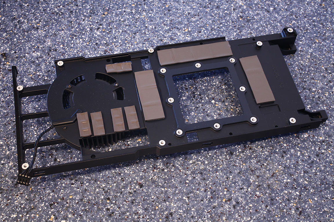
The last piece that goes off is a big black metal heatsink that covers all the "minor" components of the graphics card, like memory and voltage regulation circuitry. This approach makes it easy for water cooling and extreme cooling to be attached to the GPU only without having to worry about cooling the rest of the components.

The GTX 465 requires two 6-pin PCI-Express power connectors.

The GDDR5 memory chips are made by Samsung, and carry the model number K4G10325FE-HC05. They are specified to run at 1000 MHz (4000 MHz GDDR5 effective).
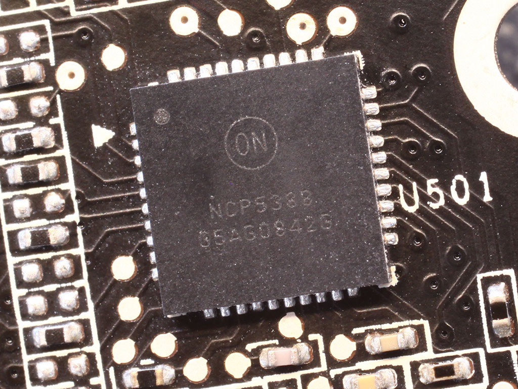
OnSemi's NCP5388 is a reasonable priced voltage regulator, unfortunately it does not have I2C voltage control. NVIDIA however exposes an API for voltage changes via VID in their NVAPI.

NVIDIA's GeForce 100 graphics processor is made on a 40 nm process at TSMC Taiwan. It uses approximately 3.2 billion transistors which makes it the most complex GPU built to-date. Please note that the silvery metal surface you see is the heatspreader of the GPU which measures 42.3 x 42.3 mm. The actual GPU die is sitting under the heatspreader, its dimensions are not known. NVIDIA did not communicate a die size measurement to the press.
May 14th, 2024 09:14 EDT
change timezone
Latest GPU Drivers
New Forum Posts
- Windows 7 Club (1025)
- Homeworld 3 [Official Thread] (38)
- not impressed - nvme vs ssd (97)
- Free Games Thread (3800)
- Purchased an AX1200i PSU as part of some forward planning, what tier is this PSU? (99)
- Having to login and enable push note every day. (5)
- Air makes its way from the reservoir into the radiator. (54)
- What's your latest tech purchase? (20521)
- Build From Old Parts (13)
- Rare GPUs / Unreleased GPUs (1886)
Popular Reviews
- Homeworld 3 Performance Benchmark Review - 35 GPUs Tested
- ZMF Caldera Closed Planar Magnetic Headphones Review
- Corsair MP700 Pro SE 4 TB Review
- ThundeRobot ML903 NearLink Review
- Upcoming Hardware Launches 2023 (Updated Feb 2024)
- AMD Ryzen 7 7800X3D Review - The Best Gaming CPU
- Bykski CPU-XPR-C-I CPU Water Block Review - Amazing Value!
- CHERRY XTRFY M64 Pro Review
- ASUS Radeon RX 7900 GRE TUF OC Review
- ASRock Radeon RX 7900 XT Phantom Gaming White Review
Controversial News Posts
- Intel Statement on Stability Issues: "Motherboard Makers to Blame" (266)
- AMD to Redesign Ray Tracing Hardware on RDNA 4 (227)
- Windows 11 Now Officially Adware as Microsoft Embeds Ads in the Start Menu (172)
- NVIDIA to Only Launch the Flagship GeForce RTX 5090 in 2024, Rest of the Series in 2025 (152)
- AMD Hits Highest-Ever x86 CPU Market Share in Q1 2024 Across Desktop and Server (122)
- Sony PlayStation 5 Pro Specifications Confirmed, Console Arrives Before Holidays (119)
- AMD's RDNA 4 GPUs Could Stick with 18 Gbps GDDR6 Memory (114)
- AMD Ryzen 9 7900X3D Now at a Mouth-watering $329 (104)