Wednesday, March 14th 2012

Inno3D GeForce GTX 560 SE Pictured

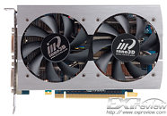
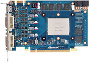
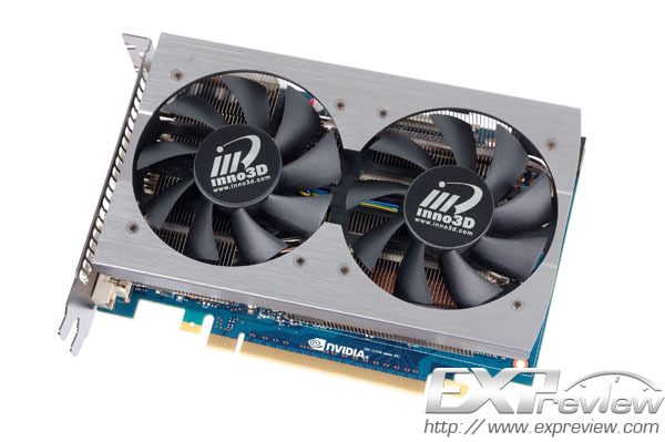
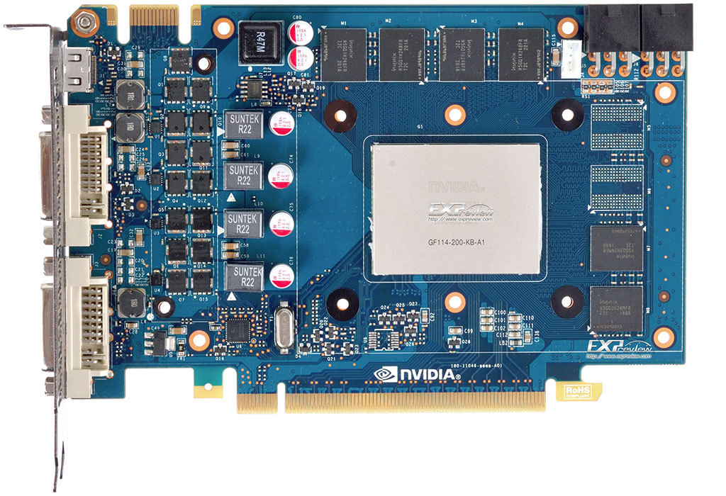
Here are some of the first pictures of Inno3D GeForce GTX 560 SE. Inno3D implemented NVIDIA's new SKU that's competitive with Radeon HD 7700 series, by designing a compact graphics card that's backed by relatively-powerful cooling. The PCB is very short (good for compact cases), and uses a simple 4+1 phase VRM to power the card. It features 1 GB of GDDR5 memory sitting on a 192-bit wide memory interface. The GTX 560 SE packs 288 CUDA cores, and clock speeds of 776/1553/953 MHz (core/CUDA cores/memory actual). Inno3D GeForce GTX 560 SE is cooled by a custom dual-slot cooling solution. This cooler makes use of two aluminum fin stacks, to which heat is conveyed by four 8 mm-thick nickel-plated copper heat pipes. The fin stacks are then ventilated by two 80 mm fans. The card has been tested at the source.
Source: Expreview
Add your own comment

7 Comments on Inno3D GeForce GTX 560 SE Pictured

#1
Shou Miko
i was wondering why, does it miss 2 memory blocks on the pcb?


does this mean this pcb was made to do more than 1024gb? maybe 1280mb or something?
Posted on Reply
#2
btarunr
Editor & Senior Moderator
puma99dk|i was wondering why, does it miss 2 memory blocks on the pcb?

does this mean this pcb was made to do more than 1024gb? maybe 1280mb or something?
<<<
Posted on Reply
#3
Shou Miko
btarunr<<<
what? maybe they r planing about make it a GTX560 Ti 488 at some points, i just think it looks weird missing 2 memory blocks ^^;

and when u think about it, if that's layout is 1024mb than the ram block will be 170,66mb pr. block and that doesn't sound right O.o
Posted on Reply
#5
ViperXTR
hint: 192bit memory interface


It uses similar memory configuration as the GTX 550 Ti:
nVidia did some modifications in the memory controller for the GTX 550 Ti, in such a way that it has three 64bit memory controllers, and each controller is controlling 2 32bit memory chips. 4 of the memory chips are 128MB in size while the remaining 2 are 256MB in size totaling 1024MB of memory at 192bit. The Raster Operators (ROP) are also tied to the memory chips, and each chip has 4 ROPs in it so in simple terms:

Note: GTX 550 Ti has 6 memory chips

Memory Controller 1 - 64bit - 128MB 32bit memory w/4 ROPs + 128MB 32bit memory w/4 ROPs
Memory Controller 2 - 64bit - 128MB 32bit memory w/4 ROPs + 128MB 32bit memory w/4 ROPs
Memory Controller 3 - 64bit - 256MB 32bit memory w/4 ROPs + 256MB 32bit memory w/4 ROPs

Total of - 192bit 1024MB memory w/ 24ROPs

In terms of memory controller, its really different from GTS 450 since it had to balance the load on the odd memory configuration, and thats up to the drivers.
Posted on Reply
#6
THE_EGG
hmm looks like there could be some turbulance between the two fans.
Posted on Reply
#7
Shou Miko
ViperXTRhint: 192bit memory interface


It uses similar memory configuration as the GTX 550 Ti:


but why mix memory sized? it doesn't make much sense to me in the end, even making a 2gig card they will just do it like that, instead of using like 256mb chips all around bcs it's cheaper to mix or bcs they don't wanna go above the bandwidth it's released with?
Posted on Reply
May 1st, 2024 10:39 EDT change timezone

New Forum Posts

Popular Reviews

Controversial News Posts