Monday, June 18th 2012

NVIDIA Tesla K10 GPU Hits New Performance Milestones For Scientific Simulation
ISC'12 - NVIDIA Tesla K10 GPUs offer performance breakthroughs on popular high performance computing (HPC) applications -- ranging from seismic processing to life sciences to video processing -- according to new benchmarks NVIDIA released today.
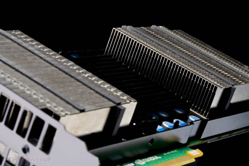
Based on the new NVIDIA Kepler computing architecture, the Tesla K10 GPU delivers the industry's highest single precision performance (4.58 teraflops) and highest memory bandwidth (320 GB/sec) in a single accelerator. This is 12 times higher single precision flops and 6.4 times higher memory bandwidth than the latest-generation Intel Sandy Bridge CPUs.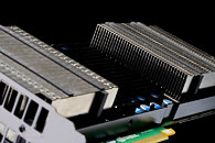 The Tesla K10 GPU outperforms CPUs and previous-generation GPUs across the board on the most popular, compute-intensive applications for four key market segments, including:
New Performance Records on AMBER and LAMMPS
On AMBER, a leading biomolecular simulation software application, four Tesla K10 GPUs achieved world record performance, delivering far superior results than what was available on multiple racks of servers just a few years ago.
The Tesla system achieved performance of 76 nanoseconds of computer simulation time in a day for a 23,558 atom molecule, outstripping the previous record set with four Tesla M2090s last year, providing supercomputing performance to thousands of individual researchers to fuel further innovation in such areas as new drug discovery and more effective materials.
"In biomolecular science, adding a few more nanoseconds of simulation time can make a world of difference in the ability of researchers to study and better understand the behavior of complex biological systems," said Ross Walker, assistant research professor, San Diego Supercomputing Center. "It still blows my mind that a single Tesla K10 outperforms some of the largest CPU clusters. The benefit it offers researchers is tremendous, enabling them to accelerate the search for new and better treatments for a host of diseases and disorders."
The Tesla K10 GPU also delivers the highest performance on LAMMPS, another application widely used by the life sciences research community. Running the LAMMPS Lennard Jones Liquid Benchmark, a single Tesla K10 GPU outperforms a Tesla M2090 GPU by 80 percent, delivering the equivalent performance of a cluster with 64 x86 CPUs.
Accelerating the Search for Energy
NVIDIA Tesla GPUs continue to deliver the highest performance on reverse time migration (RTM) applications for seismic processing in the oil and gas exploration industry, and for image processing in the computer vision industry. Petrobras, the national oil and gas company of Brazil, achieved an 1.8x speed up on its RTM application on the Tesla K10 GPU, as compared to a Tesla M2090 GPU within the same power envelope.
NVIDIA Tesla K10 GPUs are available from leading OEMs, including Appro Supercomputer Solutions, Dell, HP, IBM, SGI and Supermicro, as well as through NVIDIA distribution partners. More information about the Tesla K10 is available on the NVIDIA Tesla website.
Based on the new NVIDIA Kepler computing architecture, the Tesla K10 GPU delivers the industry's highest single precision performance (4.58 teraflops) and highest memory bandwidth (320 GB/sec) in a single accelerator. This is 12 times higher single precision flops and 6.4 times higher memory bandwidth than the latest-generation Intel Sandy Bridge CPUs.
- Defense: video analytics, video stabilization, orthorectification, computer vision
- Life and material sciences: molecular dynamics
- Oil and gas: seismic processing, reverse time migration
- Media and entertainment: video editing, video rendering/transcoding, ray tracing
New Performance Records on AMBER and LAMMPS
On AMBER, a leading biomolecular simulation software application, four Tesla K10 GPUs achieved world record performance, delivering far superior results than what was available on multiple racks of servers just a few years ago.
The Tesla system achieved performance of 76 nanoseconds of computer simulation time in a day for a 23,558 atom molecule, outstripping the previous record set with four Tesla M2090s last year, providing supercomputing performance to thousands of individual researchers to fuel further innovation in such areas as new drug discovery and more effective materials.
"In biomolecular science, adding a few more nanoseconds of simulation time can make a world of difference in the ability of researchers to study and better understand the behavior of complex biological systems," said Ross Walker, assistant research professor, San Diego Supercomputing Center. "It still blows my mind that a single Tesla K10 outperforms some of the largest CPU clusters. The benefit it offers researchers is tremendous, enabling them to accelerate the search for new and better treatments for a host of diseases and disorders."
The Tesla K10 GPU also delivers the highest performance on LAMMPS, another application widely used by the life sciences research community. Running the LAMMPS Lennard Jones Liquid Benchmark, a single Tesla K10 GPU outperforms a Tesla M2090 GPU by 80 percent, delivering the equivalent performance of a cluster with 64 x86 CPUs.
Accelerating the Search for Energy
NVIDIA Tesla GPUs continue to deliver the highest performance on reverse time migration (RTM) applications for seismic processing in the oil and gas exploration industry, and for image processing in the computer vision industry. Petrobras, the national oil and gas company of Brazil, achieved an 1.8x speed up on its RTM application on the Tesla K10 GPU, as compared to a Tesla M2090 GPU within the same power envelope.
NVIDIA Tesla K10 GPUs are available from leading OEMs, including Appro Supercomputer Solutions, Dell, HP, IBM, SGI and Supermicro, as well as through NVIDIA distribution partners. More information about the Tesla K10 is available on the NVIDIA Tesla website.
24 Comments on NVIDIA Tesla K10 GPU Hits New Performance Milestones For Scientific Simulation
They made a Tesla card out of GK 104 (in fact two GK104s) even though it sucks at computing because GK 110 ( originally meant to be the gtx 680) won't enter production any time soon.
They didn't make computing cards using GF104/GF114 because GF100 and GF110 were kick ass cards with exceptional computing performance.
and because of this they can charge more for GK110 parts since it will be amazing in both SP and DP :D
GK110's DP performance should be higher than AMD's HD7970 (according to rumors) and the new HD7970 Ghz Edition will be pretty close.
parallelis.com/k20-updated-kepler-architecture/
www.brightsideofnews.com/news/2012/5/15/nvidia-tesla-k20-ie-gk110-is-71-billion-transistors2c-300w-tdp2c-384-bit-interface.aspx
If LuxMark is any reference, then nVidia is in bad shape with Kepler.
And GK110 won't make it to Consumer markets in any case.
7.1 Billion transistor should mean a die size of roughly 600 mm square. This is extremely uneconomical for consumer markets.
................................................
But Nvidia is in for a kick-ass competition.
Intel Xeon Phi should be a larrabee core. With over 1 Teraflop of FP64 performance. It should kick K10's butt.
Edit: Also misleading to name it the K10 when it's based on a couple GK104 cores. This is NOT a GK110. IIRC, the GK110 Tesla device will be a K20.
Same ballpark as GF100.Sure - for average consumers. High-end cards are not for average consumers.
GT200 = 576mm2 / GTX 260 & 280
GF100 = 529mm2 / GTX 465, 470 & 480
GF110 = 520mm2 / GTX 560 Ti OEM, 560 TI 448, 570, 580 & 590
They seam pretty comfortable releasing chips close to 600mm2.
The problem would be how much more power it would use? AMD chip is 352mm2 and its not handy capped in computation power and is running neck and neck in power usage with the 294mm2 GK104 that is extremely hindered in that area by 2/3rds.
The ratio in Fermi was different. GF110/100 had a different ratio than GF114/104.
GK110:- 7.1 billion transistors
3.54 billion * 2 = 7.08 billion
294 mm^2 * 2 = 592 mm^2
I hope you know enough math to understand a simple calculation.
Btw there would be no use to release GK110 for consumers. Because gaming wise GTX 690 should roughly equal GK110. And since Gk110 is a much much larger die, it would consume a hell lot of power. Another factor is gonna be yields. Will TSMC cope with the pressure to produce enough 7.1 billion transistor chip? Seems unlikely till next year.
And we all know that Maxwell is coming next year(if all goes well).
3.79 TFLOPS Single Precision compute power
947 GFLOPS Double Precision compute power
the GK110 has a big ask ahead of it , if the GK104 has any input, you can double the shaders and add more Dp shaders all you like and thats still a big ask, Nvidia are using two GK104, for 4.5 Tflops SP compute power 2x 7970 would have <7.58Tflops SP compute power, in performance per watt a single 7970 must aniallate a K10 compute card.
and by the look of things we wont see the GK110 till a year after amd released the 7970.
@MrMilli
GK104's DP ratio is 1/24, not 1/16. Read the link above.