Friday, November 1st 2013

AMD to Unveil Next-Generation APUs on November 11

As a follow-up to our older article on how December-January will play out for AMD's next-generation APU lineup, we have news that the company will unveil, or at least tease its next-generation desktop APU, codename "Kaveri," on November 11, 2013. It's when the company will host its APU'13 event, modeled along the lines of GPU'13, held in Hawaii this September, where it unveiled its Radeon R9 200 and R7 200 GPU families. On its backdrop, the company will also hold its 2013 AMD Developer Summit, which brings together developers making software that take advantage of both CPU and OpenCL-accelerated GPUs. APU'13 will be held in San Jose, USA, and like GPU'13, will be live-streamed to the web. In addition to new APUs, the company is expected to make some big announcements with its HSA (heterogeneous system architecture) initiative that brought some big names in the industry on board.

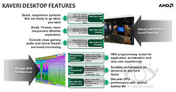
The agenda for APU'13 follows.

  • 4:00 - 5:00 p.m. (PST), Monday, November 11:
    o Lisa Su, senior vice president & general manager, Global Business Units, AMD: "Developers: The Heart of AMD Innovation"
    o Phil Rogers, corporate fellow, AMD: "The Programmers Guide to Reaching for the Cloud"
  • 8:30 - 9:30 a.m. (PST), Tuesday, November 12:
    o Mike Muller, CTO, ARM: "Is There Anything New in Heterogeneous Computing?"
    o Nandini Ramani, vice president, Java Platform, Oracle Solutions: "The Role of Java in Heterogeneous Computing, and How You Can Help"
  • 1:15 - 2:15 p.m. (PST) Tuesday, November 12:
    o Dr. Chien-Ping Lu, senior director, Mediatek USA: "How Many Cores Will We Need?"
    o Tony King-Smith, executive vice president, Marketing, Imagination Technologies: "Silicon? Check. HSA? Check. All done? Wrong!"
  • 8:30 - 9:30 a.m. (PST), Wednesday, November 13:
    o Dominic Mallinson, senior vice president, Software, Sony: "Inside PlayStation 4: Building the Best Place to Play"
    o Brendan Iribe, CEO, Oculus VR: "Virtual Reality - A New Frontier in Computing"
  • 1:15 - 2:15 p.m. (PST) Wednesday, November 13:
    o Johan Andersson, technical director, DICE: "Rendering Battlefield 4 with Mantle"
    o Mark Papermaster, CTO, AMD: "Powering the Next Generation Surround Computing Experience"
Image Credit: VR-Zone
Add your own comment

44 Comments on AMD to Unveil Next-Generation APUs on November 11

#26
TheoneandonlyMrK
dwadeAMD needs to address TDP issues for both their CPU and GPU. It's way too high, which is why they are losing to nVidia badly in the mobile market.
I find it strange that members with little to say all year can be assed throwing a little bait in Amd threads.
cheers for the input though Dwade however , this being TPU , most readers here fecked efficiency right out the window on day 1 of their new build or old rebuild when they turned Eist / cool and quite off and all other eco features off then overclocked the snot out of it and left it like that eternally or until instability shows up only to step it back a bit:confused:

MOOOOOAAAARR POWERSSSS not less pls:D
Posted on Reply
#27
ensabrenoir
flynnskifunny thing is that as bad as the reputation for the 9590s have been, Intel are no better when clocked to 5Ghz..

pctuning.tyden.cz/ilustrace3/obermaier/4770K/scaling_sandy.pngi.imgur.com/gzBNZwN.png

With Haswell things are not much better.. +18% clock costs over 60% more power (3900 to 4600mhz).. and that last 400Mhz is going to cost another 50%+ in power consumption to reach 5Ghz.
fair enough.... gotta admit though even if it was intel or nvidia in that picture.... it still would've been hilarious :laugh: And anyone who buy that level of cpu dont care about power consumption and tend to water cool so its all good
Posted on Reply
#28
HisDivineOrder
Only San Jose?

Were all the tropical island resorts taken this time, AMD?
Posted on Reply
#29
Dent1
flynnskiIn the same boat,.. X6 1100T @ 4.2Ghz, see no reason to upgrade..
I can say the same thing with an Athlon II X4 @ 3.6Ghz.
dwadeAMD needs to address TDP issues for both their CPU and GPU. It's way too high, which is why they are losing to nVidia badly in the mobile market.
Hence why AMD/ATI currently have a larger market share than Nvidia in the mobile market.
Posted on Reply
#30
Ralfies
flynnskifunny thing is that as bad as the reputation for the 9590s have been, Intel are no better when clocked to 5Ghz..

pctuning.tyden.cz/ilustrace3/obermaier/4770K/scaling_sandy.pngi.imgur.com/gzBNZwN.png

With Haswell things are not much better.. +18% clock costs over 60% more power (3900 to 4600mhz).. and that last 400Mhz is going to cost another 50%+ in power consumption to reach 5Ghz.
Not doubting the accuracy of this, but it's a little hard to take these charts seriously when they can't even spell what they're measuring.
Posted on Reply
#31
DeOdView
Dent1I can say the same thing with an Athlon II X4 @ 3.6Ghz.


Didn't we (customers) wanted our CPU to lastttt long? Funny, enough some complaint AMD socket, too! :banghead:

I gotta said, my hat is down for AMD lonnng last as good enough CPU! :respect:
Posted on Reply
#32
Dent1
DeOdViewI can say the same thing with an Athlon II X4 @ 3.6Ghz.


Didn't we (customers) wanted our CPU to lastttt long? Funny, enough some complaint AMD socket, too! :banghead:

I gotta said, my hat is down for AMD lonnng last as good enough CPU! :respect:
100% agree. When AMD was churning out CPUs they are saying slow down we just upgraded, damn corporate greed milking the consumer. Then they give us hardware which almost half a decade and people complain for something new.
RalfiesNot doubting the accuracy of this, but it's a little hard to take these charts seriously when they can't even spell what they're measuring.
Yh power "consuption". Think its the authors second language.
Posted on Reply
#33
flynnski
Dent1100% agree. When AMD was churning out CPUs they are saying slow down we just upgraded, damn corporate greed milking the consumer. Then they give us hardware which almost half a decade and people complain for something new.


Yh power "consuption". Think its the authors second language.
Iirc, the author is Czech/Slovak.. I assume that you communicate Czechoslovakian as well as they do English ???!
Posted on Reply
#34
Ralfies
flynnskiIirc, the author is Czech/Slovak.. I assume that you communicate Czechoslovakian as well as they do English ???!
I assumed as much, but that is beside the point. If I was publishing data in Czechoslovakian and trying to be taken seriously, you bet your ass I'd make sure there weren't any spelling errors. Once again, I'm not saying the data is false or inaccurate, just a little unprofessional.

Anyways, back on topic. 832 GCN cores seems like a waste of space/power if they're just going to be held back by the memory bandwidth anyways. I'm thinking it'll be between 384 and 512 cores.
Posted on Reply
#35
Dent1
flynnskiIirc, the author is Czech/Slovak.. I assume that you communicate Czechoslovakian as well as they do English ???!
Nope. But I wasn't criticising the authors spelling Ralfies was. I was just point out the mistake so everyone knew what Ralfies was talking about.
Posted on Reply
#36
flynnski
Dent1Nope. But I wasn't criticising the authors spelling Ralfies was. I was just point out the mistake so everyone knew what Ralfies was talking about.
Ahh k apologies then
Posted on Reply
#37
The Von Matrices
I'm not expecting much of anything regarding hardware announcements, even during the press conference. All the seminars involve software, and I expect that will be the theme of the conference.
RalfiesAnyways, back on topic. 832 GCN cores seems like a waste of space/power if they're just going to be held back by the memory bandwidth anyways. I'm thinking it'll be between 384 and 512 cores.
That bandwidth constraint is the issue. I don't understand why mobile processors haven't gotten wider memory buses to compensate. I can understand socketed desktop CPUs needing too many pins to support a wider memory bus, and also DIMM placement is an issue with a wide bus. But modern notebooks use BGA CPUs and soldered down memory. Theoretically a 256-bit DDR3 bus shouldn't require much more space in a laptop than a 128-bit bus, and the only increase in cost might be a PCB with a few more layers. In exchange graphics performance would scale immensely. Microsoft and Sony can do it for the APUs in their consoles and AMD's graphics division does it all the time for its GPUs, so I don't see why it isn't done for the mass market APUs.
Posted on Reply
#38
alwayssts
The Von MatricesThat bandwidth constraint is the issue. I don't understand why mobile processors haven't gotten wider memory buses to compensate. I can understand socketed desktop CPUs needing too many pins to support a wider memory bus, and also DIMM placement is an issue with a wide bus. But modern notebooks use BGA CPUs and soldered down memory. Theoretically a 256-bit DDR3 bus shouldn't require much more space in a laptop than a 128-bit bus, and the only increase in cost might be a PCB with a few more layers. In exchange graphics performance would scale immensely. Microsoft and Sony can do it for the APUs in their consoles and AMD's graphics division does it all the time for its GPUs, so I don't see why it isn't done for the mass market APUs.
You're asking the questions that have boggled my mind since the conception of the APU, and certainly what I find the most interesting challenge moving forward.

There are many conceivable answers, a wider bus among them (256-bit ddr3 would be sufficient for a ~512sp design), although perhaps less probable as we move to ddr4 and it's 1dimm-per-channel restriction and larger, more demanding iGPUs that will quickly outpace a 128-bit ddr4 bus. Certainly there is bga, but I wonder if amd is really willing to take that leap with their larger designs (as a consumer platform, ie not the ps4 or iterations of bobcat).

Hypertransport, if not a discrete (or optional) gddr5 bus to a gpu cache (ala what used to be called Sideport Memory in the discrete IGP days) seemed like a realistic option even up to this generation. While 32-bit, with the max bandwidth of a link resting somewhere near what gddr5 is capable on AMD's current gpu controllers, and meshing fairly nicely with being around half of what a 32/28nm iGPU would need (and twice what a 128-bit ddr3 bus could deliver), that would have more-or-less made sense. Obviously moving past this gen it would be less so, unless itself coupled with a ddr4 bus (ie ddr4 + gddrX).

From there, we have the possibilities of larger/faster caches (like the X1's on-die ram) offsetting what is needed externally. There is also the possibility of things like on-package off-die caches (not unlike Intel's Iris) as well stacked dram like Volta.

Whatever their solution, they need to do it yesterday. Their strength is (and has always been) in the floating point computation per mm (per process/cost) their designs deliver. While HSA capitalizes on this fact, as it should, with each passing node they lose that (realistic) advantage to intel, whom can ramp clocks higher until they reach parity in design (and then clock them lower to save power) even as their priority lies in improving their cpu cores. With each passing gpu gen nvidia grows closer to parity, as they are clearly receding from purely thinking of their designs as efficient gpus to rather more-or-less a floating point core (that makes sense as such unit with or without the shell of a cpu). The scary thing about all that is...intel and nvidia, those least dependant on memory bandwidth currently, have shown their plans for going forward. AMD, whom already is restricted on all fronts by this reality, has not (outside the ps4.)

I find that sincerely troubling. No doubt they have an answer...I just hope it comes sooner rather than later.
Posted on Reply
#39
The Von Matrices
alwaysstsYou're asking the questions that have boggled my mind since the conception of the APU, and certainly what I find the most interesting challenge moving forward.

There are many conceivable answers, a wider bus among them (256-bit ddr3 would be sufficient for a ~512sp design), although perhaps less probable as we move to ddr4 and it's 1dimm-per-channel restriction and larger, more demanding iGPUs that will quickly outpace a 128-bit ddr4 bus. Certainly there is bga, but I wonder if amd is really willing to take that leap with their larger designs (as a consumer platform, ie not the ps4 or iterations of bobcat).

Hypertransport, if not a discrete (or optional) gddr5 bus to a gpu cache (ala what used to be called Sideport Memory in the discrete IGP days) seemed like a realistic option even up to this generation. While 32-bit, with the max bandwidth of a link resting somewhere near what gddr5 is capable on AMD's current gpu controllers, and meshing fairly nicely with being around half of what a 32/28nm iGPU would need (and twice what a 128-bit ddr3 bus could deliver), that would have more-or-less made sense. Obviously moving past this gen it would be less so, unless itself coupled with a ddr4 bus (ie ddr4 + gddrX).

From there, we have the possibilities of larger/faster caches (like the X1's on-die ram) offsetting what is needed externally. There is also the possibility of things like on-package off-die caches (not unlike Intel's Iris) as well stacked dram like Volta.

Whatever their solution, they need to do it yesterday. Their strength is (and has always been) in the floating point computation per mm (per process/cost) their designs deliver. While HSA capitalizes on this fact, as it should, with each passing node they lose that (realistic) advantage to intel, whom can ramp clocks higher until they reach parity in design (and then clock them lower to save power) even as their priority lies in improving their cpu cores. With each passing gpu gen nvidia grows closer to parity, as they are clearly receding from purely thinking of their designs as efficient gpus to rather more-or-less a floating point core (that makes sense as such unit with or without the shell of a cpu). The scary thing about all that is...intel and nvidia, those least dependant on memory bandwidth currently, have shown their plans for going forward. AMD, whom already is restricted on all fronts by this reality, has not (outside the ps4.)

I find that sincerely troubling. No doubt they have an answer...I just hope it comes sooner rather than later.
From what I've read about AMD's goals, they don't want a heterogeneous memory pool like the XBOX One where different memory addresses have different bandwidths and latencies. AMD is pushing to have all memory addresses the same speed and latency in order to avoid the need for software to shuffle memory among different addresses in order to optimize bandwidth, sort of what is one with a discrete GPU today. This doesn't eliminate an algorithm implemented in the core hardware managing more levels of cache (like what Intel does with Crystalwell), but AMD wants this to be transparent to the developer.

As far as DDR4, the doubled bandwidth will stave off the bandwidth limitation for a while but even without the need for more bandwidth the 1 DIMM/channel limitation will encourage wider memory buses. The people who want lots of memory for the desktop or mobile will now need lots double the memory channels to achieve the same capacity with DDR4 as DDR3. The server market already moved in this direction with DDR3; the reason for the migration to 256-bit buses were more for the sheer memory capacity of that many memory channels rather than the increased bandwidth.
Posted on Reply
#40
NeoXF
Again people with the same concerns and mentality... *sigh*

Let me put it simple... HSA > pure iGPU for games and crap.

HSA is ment as a revolution in x86... and possibly the only thing that can save it from a slow and painful death by ARM.

Seriously, while the iGPU part should be beastly, even if with the new IMC and faster DDR3 support, it'll still come short of it's potential... the great iGPU is far from the (only) point of Kaveri...

And I'm sure, on paper at least, adding an extra 192-256 ALUs make much more performance sense to AMD, than adding 2 extra cores.
Posted on Reply
#41
Steevo
The Von MatricesFrom what I've read about AMD's goals, they don't want a heterogeneous memory pool like the XBOX One where different memory addresses have different bandwidths and latencies. AMD is pushing to have all memory addresses the same speed and latency in order to avoid the need for software to shuffle memory among different addresses in order to optimize bandwidth, sort of what is one with a discrete GPU today. This doesn't eliminate an algorithm implemented in the core hardware managing more levels of cache (like what Intel does with Crystalwell), but AMD wants this to be transparent to the developer.

As far as DDR4, the doubled bandwidth will stave off the bandwidth limitation for a while but even without the need for more bandwidth the 1 DIMM/channel limitation will encourage wider memory buses. The people who want lots of memory for the desktop or mobile will now need lots double the memory channels to achieve the same capacity with DDR4 as DDR3. The server market already moved in this direction with DDR3; the reason for the migration to 256-bit buses were more for the sheer memory capacity of that many memory channels rather than the increased bandwidth.
No, they DO want it. It improves their performance in all facets.

arstechnica.com/information-technology/2013/04/amds-heterogeneous-uniform-memory-access-coming-this-year-in-kaveri/


Instead of having software decide where to run the process from, the hardware decides in real time which is more efficient, and then runs it. Addresses are the same, so no latency penalty for transporting it around. Hugely improved performance in DSP and other filtered data, serial data still run on the CPU cores.
Posted on Reply
#42
NeoXF
Apparently AMD has indirectly confirmed the naming scheme for desktop Kaveri.


So as I suspected, Ax-7x00x. Like A10-7800K for the next top tier model.

Edit: As well as the existance of next Athlon CPUs... Like Athlon II X4 770K or 850K? I guess.
Posted on Reply
#43
The Von Matrices
SteevoNo, they DO want it. It improves their performance in all facets.

arstechnica.com/information-technology/2013/04/amds-heterogeneous-uniform-memory-access-coming-this-year-in-kaveri/

Instead of having software decide where to run the process from, the hardware decides in real time which is more efficient, and then runs it. Addresses are the same, so no latency penalty for transporting it around. Hugely improved performance in DSP and other filtered data, serial data still run on the CPU cores.
I don't understand how that article refutes what I said; I think you agree with me but didn't understand what I said. I wasn't referring to dedicated memory for the GPU and GPU, which is obviously going away. I was referring AMD not wanting something like a NUMA where different memory addresses have different bandwidths and latencies.

When programming for the XBOX One, programmers have to write their code so that the most latency and bandwidth sensitive parts are sent to the small SRAM while the rest of the data is written to the larger but slower main memory. AMD doesn't want to have developers worrying about swapping data between the SRAM versus main memory, so they want a unified memory architecture like the PS4.

This is why I don't see something like alwayssts said occurring, where there is a small, high speed, on chip cache managed by software. The whole point of AMD's heterogeneous computing initiative is to make it as easy as possible for programmers to utilize heterogeneous computing. If there is to be a large SRAM cache at all, AMD wants something more like Crystalwell where the cache is managed by hardware and it is transparent to the developer.
Posted on Reply
#44
TheoneandonlyMrK
The Von MatricesI don't understand how that article refutes what I said; I think you agree with me but didn't understand what I said. I wasn't referring to dedicated memory for the GPU and GPU, which is obviously going away. I was referring AMD not wanting something like a NUMA where different memory addresses have different bandwidths and latencies.

When programming for the XBOX One, programmers have to write their code so that the most latency and bandwidth sensitive parts are sent to the small SRAM while the rest of the data is written to the larger but slower main memory. AMD doesn't want to have developers worrying about swapping data between the SRAM versus main memory, so they want a unified memory architecture like the PS4.

This is why I don't see something like alwayssts said occurring, where there is a small, high speed, on chip cache managed by software. The whole point of AMD's heterogeneous computing initiative is to make it as easy as possible for programmers to utilize heterogeneous computing. If there is to be a large SRAM cache at all, AMD wants something more like Crystalwell where the cache is managed by hardware and it is transparent to the developer.
thats exactly it and exactly where i think they are all going, stacked chips with multi layered memory and in centralising the memory rescource it only makes sense to up the bandwidth of each route to it and remove some of the intermediary caches to bring back some latency.
Im thinking quad module for Amd but per layer and effectively 4x ddr4 imc per layer x2 for 16 logic cores from 8 tied across an 8 channel ddr4 interface to 8 gig of Tsv connected dram, drop the sytem ram too at this point and the year is,,, ,likely 2015:cool:
Posted on Reply
Add your own comment
Apr 26th, 2024 10:57 EDT change timezone

New Forum Posts

Popular Reviews

Controversial News Posts