News Posts matching #OpenCL

Return to Keyword Browsing

X-Silicon Startup Wants to Combine RISC-V CPU, GPU, and NPU in a Single Processor

While we are all used to having a system with a CPU, GPU, and, recently, NPU—X-Silicon Inc. (XSi), a startup founded by former Silicon Valley veterans—has unveiled an interesting RISC-V processor that can simultaneously handle CPU, GPU, and NPU workloads in a chip. This innovative chip architecture, which will be open-source, aims to provide a flexible and efficient solution for a wide range of applications, including artificial intelligence, virtual reality, automotive systems, and IoT devices. The new microprocessor combines a RISC-V CPU core with vector capabilities and GPU acceleration into a single chip, creating a versatile all-in-one processor. By integrating the functionality of a CPU and GPU into a single core, X-Silicon's design offers several advantages over traditional architectures. The chip utilizes the open-source RISC-V instruction set architecture (ISA) for both CPU and GPU operations, running a single instruction stream. This approach promises lower memory footprint execution and improved efficiency, as there is no need to copy data between separate CPU and GPU memory spaces.

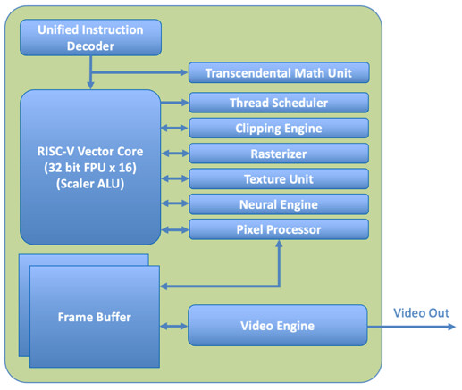
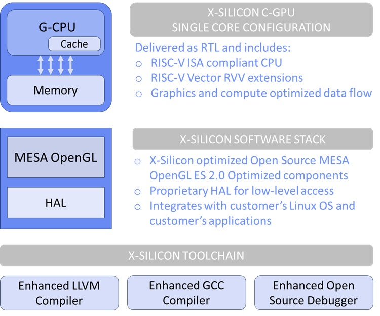
Called the C-GPU architecture, X-Silicon uses RISC-V Vector Core, which has 16 32-bit FPUs and a Scaler ALU for processing regular integers as well as floating point instructions. A unified instruction decoder feeds the cores, which are connected to a thread scheduler, texture unit, rasterizer, clipping engine, neural engine, and pixel processors. All is fed into a frame buffer, which feeds the video engine for video output. The setup of the cores allows the users to program each core individually for HPC, AI, video, or graphics workloads. Without software, there is no usable chip, which prompts X-Silicon to work on OpenGL ES, Vulkan, Mesa, and OpenCL APIs. Additionally, the company plans to release a hardware abstraction layer (HAL) for direct chip programming. According to Jon Peddie Research (JPR), the industry has been seeking an open-standard GPU that is flexible and scalable enough to support various markets. X-Silicon's CPU/GPU hybrid chip aims to address this need by providing manufacturers with a single, open-chip design that can handle any desired workload. The XSi gave no timeline, but it has plans to distribute the IP to OEMs and hyperscalers, so the first silicon is still away.

AMD Develops ROCm-based Solution to Run Unmodified NVIDIA's CUDA Binaries on AMD Graphics

AMD has quietly funded an effort over the past two years to enable binary compatibility for NVIDIA CUDA applications on their ROCm stack. This allows CUDA software to run on AMD Radeon GPUs without adapting the source code. The project responsible is ZLUDA, which was initially developed to provide CUDA support on Intel graphics. The developer behind ZLUDA, Andrzej Janik, was contracted by AMD in 2022 to adapt his project for use on Radeon GPUs with HIP/ROCm. He spent two years bringing functional CUDA support to AMD's platform, allowing many real-world CUDA workloads to run without modification. AMD decided not to productize this effort for unknown reasons but did open-source it once funding ended per their agreement. Over at Phoronix, there were several benchmarks testing AMD's ZLUDA implementation over a wide variety of benchmarks.

Benchmarks found that proprietary CUDA renderers and software worked on Radeon GPUs out-of-the-box with the drop-in ZLUDA library replacements. CUDA-optimized Blender 4.0 rendering now runs faster on AMD Radeon GPUs than the native ROCm/HIP port, reducing render times by around 10-20%, depending on the scene. The implementation is surprisingly robust, considering it was a single-developer project. However, there are some limitations—OptiX and PTX assembly codes still need to be fully supported. Overall, though, testing showed very promising results. Over the generic OpenCL runtimes in Geekbench, CUDA-optimized binaries produce up to 75% better results. With the ZLUDA libraries handling API translation, unmodified CUDA binaries can now run directly on top of ROCm and Radeon GPUs. Strangely, the ZLUDA port targets AMD ROCm 5.7, not the newest 6.x versions. Only time will tell if AMD continues investing in this approach to simplify porting of CUDA software. However, the open-sourced project now enables anyone to contribute and help improve compatibility. For a complete review, check out Phoronix tests.

Khronos Publishes Vulkan Roadmap 2024, Highlights Expanded 3D Features

Today, The Khronos Group, an open consortium of industry-leading companies creating advanced interoperability standards, announced the latest roadmap milestone for Vulkan, the cross-platform 3D graphics and compute API. The Vulkan roadmap targets the "immersive graphics" market, made up of mid- to high-end smartphones, tablets, laptops, consoles, and desktop devices. The Vulkan Roadmap 2024 milestone captures a set of capabilities that are expected to be supported in new products for that market, beginning in 2024. The roadmap specification provides a significant increase in functionality for the targeted devices and sets the evolutionary direction of the API, including both new hardware capabilities and improvements to the programming model for Vulkan developers.

Vulkan Roadmap 2024 is the second milestone release on the Vulkan Roadmap. Products that support it must be Vulkan 1.3 conformant and support the extensions and capabilities defined in both the 2022 and 2024 Roadmap specifications. Vulkan roadmap specifications use the Vulkan Profile mechanism to help developers build portable Vulkan applications; roadmap requirements are expressed in machine-readable JSON files, and tooling in the Vulkan SDK auto-generates code that makes it easy for developers to query for and enable profile support in their applications.

NVIDIA GeForce RTX 4080 SUPER GPUs Pop Up in Geekbench Browser

We are well aware that NVIDIA GeForce RTX 4080 SUPER graphics cards are next up on the review table (January 31)—TPU's W1zzard has so far toiled away on getting his evaluations published on time for options further down the Ada Lovelace SUPER food chain. This process was interrupted briefly by the appearance of custom Radeon RX 7600 XT models, but today's attention soon returned to another batch of GeForce RTX 4070 Ti SUPER cards. Reviewers are already toying around with driver-enabled GeForce RTX 4080 SUPER sample units—under strict confidentiality conditions—but the occasional leak is expected to happen. The appropriately named Benchleaks social media account has kept track of emerging test results.

The Geekbench Browser database was updated earlier today with premature GeForce RTX 4080 SUPER GPU test results—one entry highlighted by Benchleaks provides a quick look at the card's prowess in three of Geekbench 5.1's graphics API trials: Vulkan, CUDA and OpenCL. VideoCardz points out that all of the scores could be fundamentally flawed; in particular the Vulkan result of 100378 points—the regular (non-SUPER) GeForce RTX 4080 GPU can achieve almost double that figure in Geekbench 6. The SUPER's other results included a Geekbench 5 CUDA score of 309554, and an achievement of 264806 points in OpenCL. A late morning entrant looks to be hitting the right mark—an ASUS testbed (PRIME Z790-A WIFI + Intel Core i9-13900KF) managed to score 210551 points in Geekbench 6.2.2 Vulkan.

Intel Core Ultra 7 155H iGPU Outperforms AMD Radeon 780M, Comes Close to Desktop Intel Arc A380

Intel is slowly preparing to launch its next-generation Meteor Lake mobile processor family, dropping the Core i brand name in favor of Core Ultra. Today, we are witnessing some early Geekbench v6 benchmarks with the latest leak of the Core Ultra 7 155H processor, boasting an integrated Arc GPU featuring 8 Xe-Cores—the complete configuration expected in the GPU tile. This tile is also projected to be a part of the more potent Core 9 Ultra 185H CPU. The Intel Core Ultra 7 155H processor has been benchmarked in the new ASUS Zenbook 14, which houses a 16-core and 22-thread hybrid CPU configuration capable of boosting up to 4.8 GHz. Paired with 32 GB of memory, the configuration was well equipped to supply CPU and GPU with sufficient memory space.

Perhaps the most interesting information from the submission was the OpenCL score of the GPU. Clocking in at 33948 points in Geekbench v6, the GPU is running over AMD's Radeon 780M GPU found in APU solutions like AMD Ryzen 9 7940HS and Ryzen 9 7940U, which scored 30585 and 27345 points in the same benchmark, respectively. The GPU tile is millimeters away from closing the gap between itself and the desktop Intel Arc A380 discrete GPU, which scored 37105 points for less than a 10% difference. The Xe-LPG GPU version is bringing some interesting performance points for the integrated GPU platform, which means that Intel's Meteor Lake SKUs will bring more performance/watt than ever.

AMD Radeon PRO W7600 GPU Spotted in Geekbench Database

An interesting system popped up on Geekbench Browser early this morning—on initial inspection the evaluated high-end PC was sporting hardware of 2021-vintage, but its graphics card was observed as an outlier. The Intel Core i9-12900K (Alder Lake-S) CPU was sitting on an MSI MPG Z690 Carbon WiFi mainboard, with 64 GB of DDR5 SDRAM (3990 MT/s). The benchmarked computer was running Microsoft Windows 11 Pro (64-bit) on a power saver (economizador) plan. According to the entry's OpenCL information section we are looking at an attached GPU device called "GFX1102 ID," the board name is revealed to be "AMD Radeon PRO W7600" with 8 GB of VRAM. This lower-end alternative to existing (RDNA 3) Radeon Pro models—W7900 (48 GB) and W7800 (32 GB)—could be nearing a public launch.

This information aligns the workstation-oriented card with AMD's Navi 33 GPU—the same GFX1102 designation appears within TPU's database entry (look at the Shader ISA (GFX11.0) graphics feature). VideoCardz reckons that the leaked Radeon PRO W7600 is closely related to AMD's mobile Radeon RX 7700/7600 series—based on Navi 33, due to their matching IDs. Their report proposed: "Based on this data, the GPU is expected to have a clock speed of 1940 MHz. Comparatively, this is 310 MHz lower than the Radeon RX 7600 gaming model, which refers to its Game Clock of 2250 MHz. The Compute Unit field refers to "Workgroup Processor/WGP" cluster, so the card features 32 Compute Units or 2048 Stream Processors, the same configuration as the RX 7600. The card is listed with 8 GB of memory, but it remains uncertain whether this model will support ECC (error correction), a feature found in the W7900/W7800 models. It's important to note that the W6600 did not utilize this type of memory."

Imagination GPUs Gains OpenGL 4.6 Support

When it comes to APIs, OpenGL is something of a classic. According to the Khronos Group, OpenGL is the most widely adopted 2D and 3D graphics API. Since its launch in 1992 it has been used extensively by software developers for PCs and workstations to create high-performance, visually compelling graphics applications for markets such as CAD, content creation, entertainment, game development and virtual reality.

To date, Imagination GPUs have natively supported OpenGL up until Release 3.3 as well as OpenGL ES (the version of OpenGL for embedded systems), Vulkan (a cross-platform graphics API) and OpenCL (an API for parallel programming). However, thanks to the increasing performance of our top-end GPUs, especially with the likes of the DXT-72-2304, they present a competitive offering to the data centre and desktop (DCD) market. Indeed, we have multiple customers - including the likes of Innosilicon - choosing Imagination GPUs for the flexibility an IP solution, their scalability and their ability to offer up to 6 TFLOPS of compute.

Intel to Introduce Core Ultra Brand Extension with "Meteor Lake," iGPU Packs 128 EU

Intel is planning a major change in its client processor brand extensions with its next-generation mobile processors codenamed "Meteor Lake." The company is working to introduce the new Core Ultra brand extensions, where "Ultra" replaces the "i" in extensions such as i3, i5, i7, and i9 in some processor models. An example of such a brand extension would be the "Core Ultra 5 1003H." Ashes of the Singularity benchmark leaks of the processors surfaced on social media.

The benchmark also detects 128 EU (1,024 unified shaders) for the iGPU powering "Meteor Lake." If true, this iGPU could offer performance that's in the league of an Arc A380 discrete GPU, with some performance lost to the shared memory setup compared to the A380 with its dedicated graphics memory. The iGPU clock speed is detected to be 2.10 GHz, and having 4 MB of L2 cache, the last-level cache local to the Graphics Tile. The detection string for the iGPU as reported by its OpenCL ICD reads "Intel(R) Graphics i gfx-driver-ci-master-13736 DCH RI (1024S 128C SM3.0 2.1GHz, 4MB L2, 12.7GB)."

Mobileye Launches EyeQ Kit: New SDK for Advanced Safety and Driver-Assistance Systems

Mobileye, an Intel company, has launched the EyeQ Kit - its first software development kit (SDK) for the EyeQ system-on-chip that powers driver-assistance and future autonomous technologies for automakers worldwide. Built to leverage the powerful and highly power-efficient architecture of the upcoming EyeQ 6 High and EyeQ Ultra processors, EyeQ Kit allows automakers to utilize Mobileye's proven core technology, while deploying their own differentiated code and human-machine interface tools on the EyeQ platform.

"EyeQ Kit allows our customers to benefit from the best of both worlds — Mobileye's proven and validated core technologies, along with their own expertise in delivering unique driver experiences and interfaces. As more core functions of vehicles are defined in software, we know our customers will want the flexibility and capacity they need to differentiate and define their brands through code."
- Prof. Amnon Shashua, Mobileye president and chief executive officer

Moore Threads Unveils MTT S60 & MTT S2000 Graphics Cards with DirectX Support

Chinese company Moore Threads has unveiled their MTT GPU series just 18 months after the company's establishment in 2020. The MT Unified System Architecture (MUSA) architecture is the first for any Chinese company to be developed fully domestically and includes support for DirectX, OpenCL, OpenGL, Vulkan, and CUDA. The company announced the MTT S60 and MTT S2000 single slot desktop graphics cards for gaming and server applications at a recent event. The MTT S60 is manufactured on a 12 nm node and features 2,048 MUSA cores paired with 8 GB of LPGDDR4X memory offering 6 TFLOPs of performance. The MTT S2000 is also manufactured on a 12 nm node and doubles the number of MUSA cores to 4096 paired with 32 GB of undisclosed video memory allowing it to reach 12 TFLOPs.

Moore Threads joins Intel in supporting AV1 encoding on a consumer GPU with MUSA cards featuring H.264, H.265, and AV1 encoding support in addition to H.264, H.265, AV1, VP8, and VP9 decoding. The company is also developing a physics engine dubbed Alphacore which is said to work with existing tools such as Unity, Unreal Engine, and Houdini to accelerate physics performance by 5 to 10 times. The only gaming performance shown was a simple demonstration of the MTT S60 running League of Legends at 1080p without any frame rate details.

NVIDIA MX550 Rumored to Feature GA107 GPU with 2 GB of GDDR6 memory

The NVIDIA MX550 has allegedly surfaced as part of a new Lenovo laptop in a Geekbench listing paired with an Intel Core i7-1260P 12 core, 16 thread processor. The card is described as a "Graphics Device" in the Geekbench listing however according to ITHome this is actually the upcoming MX550 entry-level mobile graphics card. The card is supposedly based on the Ampere GA107 GPU with 16 Compute Units and 128 CUDA cores paired with 2 GB of GDDR6 memory. The MX550 is the successor to the MX450 launched in August 2020 and should offer a roughly 15% performance increase according to the Geekbench OpenCL score. We have limited information on the availability of the card or the remainder of the MX500 series except that NVIDIA may officially announce them sometime early next year.

Chinese Innosilicon Fenghua No.1 Graphics Card Supports PCIe 4.0, HDMI 2.1, GDDR6X, & DirectX

Chinese company Innosilicon Technology has recently announced their Fenghua No.1 high-performance server graphics card. The card features a dual-fan cooling design with HDMI 2.1 and Embedded DisplayPort 1.4 video connectors. The card will utilize a PCIe 4.0 connector and features GDDR6X memory developed by Innosilicon Technology with potential speeds of 21 Gbps. We have seen announcements from Chinese companies with similar products in the past but this recent announcement is the first to include support for a variety of graphics APIs including DirectX. The press release from the company didn't specify the DirectX version supported but also noted that the card will support OpenGL, OpenGLES, OpenCL, and Vulkan which will enable VR, AR, and AI applications.

AMD Radeon PRO V620 GPU Delivers Powerful, Multi-Purpose Data Center Visual Performance for Today's Demanding Cloud Workloads

AMD announced the AMD Radeon PRO V620 GPU, built with the latest AMD RDNA 2 architecture which delivers high-performance GPU acceleration for today's demanding cloud workloads including immersive AAA game experiences, intensive 3D workloads and modern office productivity applications at scale in the cloud.

With its innovative GPU-partitioning capabilities, multi-stream hardware accelerated encoders and 32 GB GDDR6 memory, the AMD Radeon PRO V620 offers dedicated GPU resources that scale to multiple graphics users, helping ensure cost-effective graphics acceleration for a range of workloads. Built using the same GPU architecture that powers the latest generation game consoles and PC game experiences, the AMD Radeon PRO V620 GPU is also designed to develop and deliver immersive AAA game experiences.

Jingjia Micro JM9 GPU Series Targeting GTX 1080 Performance Tapes Out

The Chinese Electronics company Jingjia Micro have recently completed the tapeout of their JM9 GPU series almost 2 years after they first announced the lineup. The JM9 series will consist of two GPUs with the entry-level JM9231 targeting GTX 1050 performance while the higher-end JM9271 aims for the GTX 1080. The JM9231 is stated to feature a clock speed above 1.5 GHz, 8 GB of GDDR5 memory, and will provide 2 TFLOPS of performance within a 150 W TDP through a PCIe Gen3 x16 interface. The JM9271 increases the clock speed to above 1.8 GHz and is paired with 16 GB of HBM memory which should offer 8 TFLOPS of single-precision performance to rival the GTX 1080. The card manages to do this within a TDP package of 200 W and also includes PCIe Gen4 x16 support. The two cards both support HDMI 2.0 in addition to DisplayPort 1.3 for the JM9231 and DisplayPort 1.4 for the JM9271.

While the JM9271 may target GTX 1080 performance it only features OpenGL and OpenCL API support lacking DirectX or Vulkan compatibility greatly reducing its use for gaming. The cards were originally expected to be available in 2020 but after various delays they are now ready to enter production. These products are highly unlikely to make their way outside of the Chinese mainland and if they did we wouldn't expect them to have much impact on the global market.

Hackers Innovate Way to Store and Execute Malware from Video Memory to Evade Anti-Malware

Cybercriminals have innovated a way to store malware code inside GPU dedicated memory (video memory), and execute code directly from there. Execution from video memory may not be new, but they've mostly been confined to the academic space, and unrefined. This would be the first time a proof-of-concept of a working tool that injects executables to video memory, surfaced on a hacker forum.

The tool relies on OpenCL 2.0, and its developers claim to have successfully tested it on Intel Gen9, AMD RDNA, NVIDIA Kepler, and NVIDIA Turing graphics architectures (i.e. UHD 620, UHD 630, Radeon RX 5700, GeForce GTX 740M, and GTX 1650). What makes this ingenious is that the malware binary is stored entirely in GPU memory address-space and is executed by the GPU, rather than the CPUs. Conventional anti-malware software are only known to scan the system memory, disks, and network traffic for malware; but not video memory. Hopefully this will change.

Intel DG2 GPU with 256 Execution Units Offers GTX 1050 Performance

We have been receiving several leaks for Intel's upcoming DG2 GPUs with a 256 Execution Unit model recently appearing on Geekbench paired with a 14-core Alder Lake mobile CPU. The Alder Lake mobile processor featured an integrated Xe GPU with 96 Execution Units which were also benchmarked. The 256 Execution Unit graphics card tested is likely derived from the mid-range DG2-384 GPU. The 96 EU DG2 iGPU featured a maximum frequency of 1.2 GHz while the 256 EU variant increased that to 1.4 GHz. The DG2-256 scored an OpenCL score of 18,450 points in the Geekbench 5 benchmark which places it at GTX 1050 performance level. The DG2-96 integrated GPU scored 6,500 points which is comparable to a GTX 460. While these performance numbers are low it is important to keep in mind that these are just early results from a mid-range mobile offering and Intel is planning to release cards with 512 Execution Units which should compete with the RTX 3070 Ti and 6700 XT.

GPU Memory Latency Tested on AMD's RDNA 2 and NVIDIA's Ampere Architecture

Graphics cards have been developed over the years so that they feature multi-level cache hierarchies. These levels of cache have been engineered to fill in the gap between memory and compute, a growing problem that cripples the performance of GPUs in many applications. Different GPU vendors, like AMD and NVIDIA, have different sizes of register files, L1, and L2 caches, depending on the architecture. For example, the amount of L2 cache on NVIDIA's A100 GPU is 40 MB, which is seven times larger compared to the previous generation V100. That just shows how much new applications require bigger cache sizes, which is ever-increasing to satisfy the needs.

Today, we have an interesting report coming from Chips and Cheese. The website has decided to measure GPU memory latency of the latest generation of cards - AMD's RDNA 2 and NVIDIA's Ampere. By using simple pointer chasing tests in OpenCL, we get interesting results. RDNA 2 cache is fast and massive. Compared to Ampere, cache latency is much lower, while the VRAM latency is about the same. NVIDIA uses a two-level cache system consisting out of L1 and L2, which seems to be a rather slow solution. Data coming from Ampere's SM, which holds L1 cache, to the outside L2 is taking over 100 ns of latency.

Intel Alder Lake Processor Tested, Big Cores Ramp Up to 3 GHz

Intel "Alder Lake" is the first processor generation coming from the company to feature the hybrid big.LITTLE type core arrangement and we are wondering how the configurations look like and just how powerful the next-generation processors are going to be. Today, a Geekbench submission has appeared that gave us a little more information about one out of twelve Alder Lake-S configurations. This time, we are getting an 8-core, 16-threaded design with all big cores and no smaller cores present. Such design with no little cores in place is exclusive to the Alder Lake-S desktop platform, and will not come to the Alder Lake-P processors designed for mobile platforms.

Based on the socket LGA1700, the processor was spotted running all of its eight cores at 2.99 GHz frequency. Please note that this is only an engineering sample and the clock speeds of the final product should be higher. It was paired with the latest DDR5 memory and NVIDIA GeForce RTX 2080 GPU. The OpenCL score this CPU ran has shown that it has provided the GPU with more than enough performance. Typically, the RTX 2080 GPU scores about 106101 points in Geekbench OpenCL tests. Paired with the Alder Lake-S CPU, the GPU has managed to score as much as 108068 points, showing the power of the new generation of cores. While there is still a lot of mystery surrounding the Alder Lake-S series, we have come to know that the big cores used are supposed to be very powerful.

EIZO Releases Rugged XMC GPGPU Card for Media Applications

EIZO Rugged Solutions Inc., a provider of ruggedized graphics and video products, has released the Condor NVP2009AxX - an XMC graphics and GPGPU card that supports various combinations of analog and digital outputs.

The new high-performance graphics card based on the NVIDIA Quadro P2000 GPU (chip-down GP107) supports four field customizable video output combinations of DisplayPort++, 3G-SDI, CVBS (NTSC/PAL/SECAM), and VGA (STANAG 3350, RS-170, RS-343) to provide flexibility and simplify inventory management for high-end surveillance customers. With multiple I/O configurations, the card can support a range of video resolutions up to 4K and custom resolutions under VGA configurations. It can be factory configured to customer specifications and/or field programmed to support complex, multi-video needs after deployment.

NVIDIA GeForce RTX 3080 Mobile Maxes Out "GA104" Silicon

With the desktop GeForce RTX 3080 being based on the "big" GeForce Ampere silicon, the "GA102," we wondered how NVIDIA would go about designing the RTX 3080 Mobile. It turns out that the company will max out the smaller "GA104" silicon on which the desktop RTX 3070 and RTX 3060 Ti, are based. An unreleased ASUS ROG Zephyrus Duo (GX551QS) gaming notebook's Geekbench online database entry reveals the name-string and streaming multiprocessor (SM) count of the RTX 3080 Mobile.

The Geekbench online database entry lists out the OpenCL device (GPU) name-string as "GeForce RTX 3080 Laptop GPU," and OpenCL compute unit (SM) count as 48. This corresponds with the maximum SM count of the "GA104," which features 6,144 Ampere CUDA cores spread across 24 TPCs (48 SM), 48 2nd generation RT cores, 192 3rd generation Tensor cores, 192 TMUs, and 96 ROPs. The Geekbench entry also reveals the video memory amount as 16 GB, maxing out the 256-bit wide GDDR6 memory interface of the "GA104," likely using 16 Gbit memory chips.

AMD Radeon RX 6900 XT Graphics Card OpenCL Score Leaks

AMD has launched its RDNA 2 based graphics cards, codenamed Navi 21. These GPUs are set to compete with NVIDIA's Ampere offerings, with the lineup covering the Radeon RX 6800, RX 6800 XT, and RX 6900 XT graphics cards. Until now, we have had reviews of the former two, but not the Radeon RX 6900 XT. That is because the card is coming at a later date, specifically on December 8th, in just a few days. As a reminder, the Radeon RX 6900 XT GPU is a Navi 21 XTX model with 80 Compute Units that give a total of 5120 Stream Processors. The graphics card uses a 256-bit bus that connects the GPU with 128 MB of its Infinity Cache to 16 GB of GDDR6 memory. When it comes to frequencies, it has a base clock of 1825 MHz, with a boost speed of 2250 MHz.

Today, in a GeekBench 5 submission, we get to see the first benchmarks of AMD's top-end Radeon RX 6900 XT graphics card. Running an OpenCL test suite, the card was paired with AMD's Ryzen 9 5950X 16C/32T CPU. The card managed to pass the OpenCL test benchmarks with a score of 169779 points. That makes the card 12% faster than RX 6800 XT GPU, but still slower than the competing NVIDIA GeForce RTX 3080 GPU, which scores 177724 points. However, we need to wait for a few more benchmarks to appear to jump to any conclusions, including the TechPowerUp review, which is expected to arrive once NDA lifts. Below, you can compare the score to other GPUs in the GeekBench 5 OpenCL database.

AMD Radeon RX 6800 and RX 6800 XT GPU OpenCL Performance Leaks

AMD has just recently announced its next-generation Radeon RX 6000 series GPU based on the new RDNA 2 architecture. The architecture is set to compete with NVIDIA Ampere architecture and highest offerings of the competing company. Today, thanks to the well-known leaker TUM_APISAK, we have some Geekbench OpenCL scores. It appears that some user has gotten access to the system with the Radeon RX 6800 and RX 6800 XT GPUs, running Cinebench 4.4 OpenCL tests. In the tests, the system ran on the Intel platform with Core i9-10900K CPU with 16 GB DDR4 RAM running at 3600 MHz. The motherboard used was ASUS top-end ROG Maximus XII Extreme Z490 board.

When it comes to results, the system with RX 6800 GPU scored anywhere from 347137 points to 336367 points in three test runs. For comparison, NVIDIA GeForce RTX 3070 scores about 361042 points, showcasing that the Radeon card is not faster in any of the runs. When it comes to the higher-end Radeon RX 6800 XT GPU, it scored 407387 and 413121 points in two test runs. Comparing that to GeForce RTX 3080 GPU that scores 470743 points, the card is slower compared to the competition. There has been a Ryzen 9 5950X test setup that boosted the performance of Radeon RX 6800 XT card by quite a lot, making it reach 456837 points, making a huge leap over the Intel-based system thanks to the Smart Access Memory (SAM) technology that all-AMD system provides.

Intel Xe-HP "NEO Graphics" GPU with 512 EUs Spotted

Intel is preparing to flood the market with its Xe GPU lineup, covering the entire vector from low-end to high-end consumer graphics cards. Just a few days ago, the company has announced its Iris Xe MAX GPU, the first discrete GPU from Intel, aimed at 1080p gamer and content creators. However, that seems to be only the beginning of Intel's GPU plan and just a small piece of the entire lineup. Next year, the company is expected to launch two GPU families - Xe-HP and Xe-HPG. With the former being a data-centric GPU codenamed Arctic Sound, and the latter being a gaming-oriented GPU called DG2. Today, thanks to the GeekBench listing, we have some information on the Xe-HP GPU.

Being listed with 512 EUs (Execution Units), translating into 4096 shading units, the GPU is reportedly a Xe-HP variant codenamed "NEO Graphics". This is not the first time that the NEO graphics has been mentioned. Intel has called a processor Neo graphics before, on its Architecture day when the company was demonstrating the FP32 performance. The new GeekBench leak shows the GPU running at 1.15 GHz clock speed, where at the Architecture day the same GPU ran at 1.3 GHz frequency, indicating that this is only an engineering sample. The GPU ran the GeekBench'es OpenCL test and scored very low 25,475 points. Compared to NVIDIA's GeForce RTX 3070 GPU that scored 140,484, the Intel GPU is at least four times slower. That is possibly due to the non-optimization of the benchmark, which could greatly improve in the future. In the first picture below, this Xe-HP GPU would represent the single-tile design.

Khronos Group Releases SYCL 2020 Provisional Specification

Today, The Khronos Group, an open consortium of industry-leading companies creating graphics and compute interoperability standards, announces the ratification and public release of the SYCL 2020 Provisional Specification. SYCL is a standard C++ based heterogeneous parallel programming framework for accelerating High Performance Computing (HPC), machine learning, embedded computing, and compute-intensive desktop applications on a wide range of processor architectures, including CPUs, GPUs, FPGAs, and AI processors.The SYCL 2020 Provisional Specification is publicly available today to enable feedback from developers and implementers before the eventual specification finalization and release of the SYCL 2020 Adopters Program, which will enable implementers to be officially conformant—tentatively expected by the end of the year.

A royalty-free open standard, SYCL 2020 enables significant programmer productivity through an expressive domain-specific language, compact code, and simplified common patterns, such as Class Template Argument Deduction and Deduction Guides, all while preserving significant backwards compatibility with previous versions. SYCL 2020 is based on C++17 and includes new programming abstractions, such as unified shared memory, reductions, group algorithms, and sub-groups to enable high-performance applications across diverse hardware architectures.

AMD EPYC Scores New Supercomputing and High-Performance Cloud Computing System Wins

AMD today announced multiple new high-performance computing wins for AMD EPYC processors, including that the seventh fastest supercomputer in the world and four of the 50 highest-performance systems on the bi-annual TOP500 list are now powered by AMD. Momentum for AMD EPYC processors in advanced science and health research continues to grow with new installations at Indiana University, Purdue University and CERN as well as high-performance computing (HPC) cloud instances from Amazon Web Services, Google, and Oracle Cloud.

"The leading HPC institutions are increasingly leveraging the power of 2nd Gen AMD EPYC processors to enable cutting-edge research that addresses the world's greatest challenges," said Forrest Norrod, senior vice president and general manager, data center and embedded systems group, AMD. "Our AMD EPYC CPUs, Radeon Instinct accelerators and open software programming environment are helping to advance the industry towards exascale-class computing, and we are proud to strengthen the global HPC ecosystem through our support of the top supercomputing clusters and cloud computing environments."
Return to Keyword Browsing
Apr 26th, 2024 20:40 EDT change timezone

New Forum Posts

Popular Reviews

Controversial News Posts