Monday, January 20th 2014

AMD A10-7700K "Kaveri" De-lidded

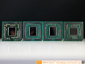
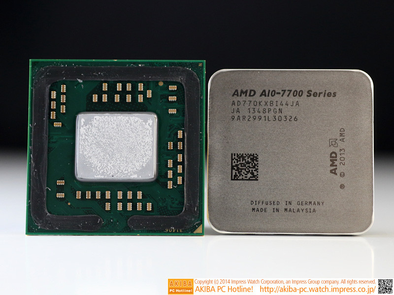
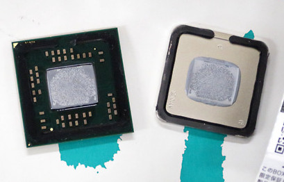
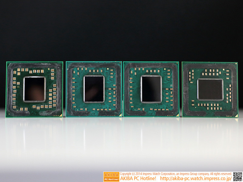
Here are the first pictures of an AMD A10-7700K "Kaveri" APU with its integrated heat-spreader (IHS, or 'lid') removed. Put next to its predecessors, "Richland," "Trinity," and "Llano," AMD's new APU silicon is its biggest for the DIY PC market, more so because it's built on the 28 nm silicon fab process, compared to its predecessors being built on 32 nm. The die measures roughly 245 mm², and packs a staggering 2.41 billion transistors.

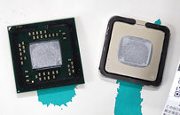
Under the IHS, AMD is using a thermal paste to transport heat from the die, and not a solder. The chip should be easy to de-lid, if you know what you're doing. Kaveri integrates two "Steamroller" x86-64 CPU modules with two cores each, a total of 4 MB of L2 cache, a massive on-die GPU with 512 stream processors based on the Graphics CoreNext micro-architecture, a dual-channel DDR3 IMC with hUMA and DDR3-2400 native support; and a PCI-Express 3.0 root complex.
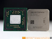
Source: Akiba PC Hotline
Add your own comment

27 Comments on AMD A10-7700K "Kaveri" De-lidded

#1
wotevajjjj
Did they leave a part unglued to make delidding easier or is there another reason ?
Cant wait to get my hammer out again
Posted on Reply
#2
RCoon
wotevajjjjDid they leave a part unglued to make delidding easier or is there another reason ?
Cant wait to get my hammer out again
They're doing it to save money, no other reason. Intel did it and got away with it, therefore so shall AMD.
Posted on Reply
#3
Vario
What are the long term prospects with that? Can the intel or amd thermal paste dry out under the lid?
Posted on Reply
#4
Fourstaff
VarioWhat are the long term prospects with that? Can the intel or amd thermal paste dry out under the lid?
I don't think so, since most thermal pastes I have come across doesn't dry out. Maybe in extreme circumstances though.
Posted on Reply
#5
RCoon
VarioWhat are the long term prospects with that? Can the intel or amd thermal paste dry out under the lid?
When I delidded my 3570K, I had to repaste the IHS every 6 months because the TIM baked itself (MX-5), and temperatures just got worse over time. Not inoperable-worse, but a couple of degrees worse. Enough to screw up clocks at the far end of the spectrum after a few months of use.
Posted on Reply
#6
iO
wotevajjjjDid they leave a part unglued to make delidding easier or is there another reason ?
Looks like a vent hole to prevent a pressure built-up due to expanding air when the CPU heats up.
Posted on Reply
#7
TheGuruStud
So long SOI. I do not welcome our shitty, new silicon overlord.
Posted on Reply
#8
buildzoid
TheGuruStudSo long SOI. I do not welcome our shitty, new silicon overlord.
I hope the next FX processors are still on 32nm SOI because this 28nm stuff doesn't clock at all 4.5Ghz average on HWbot right now and 4.8Ghz required over 1.55v sure these are 10% faster per clock but if they clock that much worse it really doesn't matter because 4.8Ghz x1.1 is equal to the 32nm SOI stuff running at 5.28Ghz which isn't very rare, d1nky even got his FX8350 all the way to 5.7Ghz on water cooling.
As of right now the best process for OCing has got to be 32nm SOI(good on air water and LN2) and the worst is intel's 22nm(terrible on air/water ok on LN2) but this 28nm stuff might still be even worse.
Posted on Reply
#9
TheGuruStud
buildzoidI hope the next FX processors are still on 32nm SOI because this 28nm stuff doesn't clock at all 4.5Ghz average on HWbot right now and 4.8Ghz required over 1.55v sure these are 10% faster per clock but if they clock that much worse it really doesn't matter because 4.8Ghz x1.1 is equal to the 32nm SOI stuff running at 5.28Ghz which isn't very rare, d1nky even got his FX8350 all the way to 5.7Ghz on water cooling.
As of right now the best process for OCing has got to be 32nm SOI(good on air water and LN2) and the worst is intel's 22nm(terrible on air/water ok on LN2) but this 28nm stuff might still be even worse.
Yep, glofo keeps talking a big game about fd-soi but no one's rich or ballsy enough to use it (that we care about).
Posted on Reply
#10
newtekie1
Semi-Retired Folder
RCoonThey're doing it to save money, no other reason. Intel did it and got away with it, therefore so shall AMD.
Actually, it is there to allow gasses and pressure to escape while the epoxy cures. Everything with an IHS has an opening for this function, the old P4's used to have a hole in the IHS to allow this, but everyone has now switched to leaving a small gap in the epoxy.
Posted on Reply
#11
Freedom4556
newtekie1Actually, it is there to allow gasses and pressure to escape while the epoxy cures. Everything with an IHS has an opening for this function, the old P4's used to have a hole in the IHS to allow this, but everyone has now switched to leaving a small gap in the epoxy.
I think he was referring to Doh, can't read. The switch from solder to paste is very unfortunate, IMO, because this only hurts the kind of people who are buying APUs in the first place: mainstream and budget.

And btw, the LGA 775 P4s had already switched to the vent slot. The hole was only for socket 478 P4s like Northwood:
Compared to:
Posted on Reply
#12
Vario
RCoonWhen I delidded my 3570K, I had to repaste the IHS every 6 months because the TIM baked itself (MX-5), and temperatures just got worse over time. Not inoperable-worse, but a couple of degrees worse. Enough to screw up clocks at the far end of the spectrum after a few months of use.
I had the same experience and I traded it for a 2550k.
Posted on Reply
#13
xorbe
Can the high temp paste be carefully salvaged from within and reused with direct core contact?
Posted on Reply
#14
Steevo
Solder is better for conductivity, but a good TIM can be made to perform a phase change with a high temp application during IHS installation and never again under normal operating temps.
Posted on Reply
#15
newtekie1
Semi-Retired Folder
Freedom4556The switch from solder to paste is very unfortunate, IMO, because this only hurts the kind of people who are buying APUs in the first place: mainstream and budget.
How does this hurt them? The paste will work just fine for people in the mainstream and budget area. Also, I'm pretty sure all the FM2 processors used paste and not solder.
Posted on Reply
#16
OC-Rage
WOOOOOOOOOOOOOOOOOOOOOOWc 2.41 billion transistors
Posted on Reply
#17
RCoon
newtekie1Actually, it is there to allow gasses and pressure to escape while the epoxy cures. Everything with an IHS has an opening for this function, the old P4's used to have a hole in the IHS to allow this, but everyone has now switched to leaving a small gap in the epoxy.
Whatever you're talking about is not what I was talking about ...
Posted on Reply
#18
newtekie1
Semi-Retired Folder
RCoonWhatever you're talking about is not what I was talking about ...
I was talking about the gap in the epoxy, what wotevajjjj asked about. What were you talking about. and what does it have to do with what wotevajjjj asked?
Posted on Reply
#19
RCoon
newtekie1I was talking about the gap in the epoxy, what wotevajjjj asked about. What were you talking about. and what does it have to do with what wotevajjjj asked?
You quoted me when replying about epoxy, i was talking about the use of TIM between IHS and physical die.
Posted on Reply
#20
newtekie1
Semi-Retired Folder
RCoonYou quoted me when replying about epoxy, i was talking about the use of TIM between IHS and physical die.
Go read wotevajjjj's post that you quoted again. He is talking about why they left the part unglued, why there is a gap in the epoxy, you said it was to save money. Sorry for the misunderstanding, but it seemed like you were talking about the epoxy, since that is what wotevajjjj was talking about.
Posted on Reply
#21
RCoon
newtekie1Go read wotevajjjj's post that you quoted again. He is talking about why they left the part unglued, why there is a gap in the epoxy, you said it was to save money. Sorry for the misunderstanding, but it seemed like you were talking about the epoxy, since that is what wotevajjjj was talking about.
I don't honestly know how I deviated so far from what he was asking :laugh:
Posted on Reply
#22
newtekie1
Semi-Retired Folder
RCoonI don't honestly know how I deviated so far from what he was asking :laugh:
It happens, the TIM issue was in the OP, so you probably just had it in your mind.
Posted on Reply
#23
grndzro7
Intel used crap TP with Ivy bridge. That's why the performance was crap.
Soldered lids do not have 100% surface contact. A good TP can actually provide better temperatures than Solder because of greater surface area.
Posted on Reply
#24
Freedom4556
newtekie1How does this hurt them? The paste will work just fine for people in the mainstream and budget area. Also, I'm pretty sure all the FM2 processors used paste and not solder.
grndzro7Intel used crap TP with Ivy bridge. That's why the performance was crap.
Soldered lids do not have 100% surface contact. A good TP can actually provide better temperatures than Solder because of greater surface area.
This is what I was getting at. If they use crap TP and it hurts overclocking, this will only affect people with no interest in de-lidding or replacing the TIM every 6 months. I suppose it makes no difference to stock performance.
Posted on Reply
#25
suraswami
RCoonWhen I delidded my 3570K, I had to repaste the IHS every 6 months because the TIM baked itself (MX-5), and temperatures just got worse over time. Not inoperable-worse, but a couple of degrees worse. Enough to screw up clocks at the far end of the spectrum after a few months of use.
Thats because you delidded and applied paste during winter and 6 months past it's Summer :p
Posted on Reply
Add your own comment
Apr 27th, 2024 06:39 EDT change timezone

New Forum Posts

Popular Reviews

Controversial News Posts