Wednesday, February 12th 2014

GTX 750 Taken Apart, Sips Power from a Single 6-pin Connector

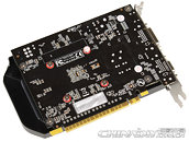
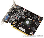
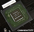
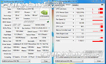
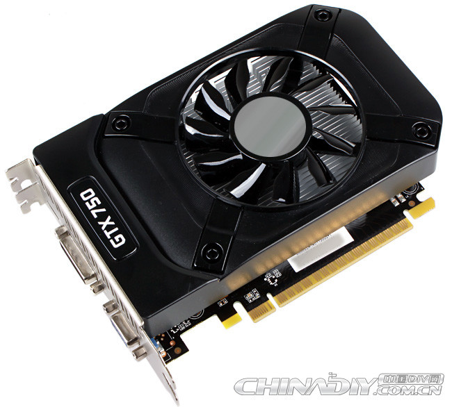
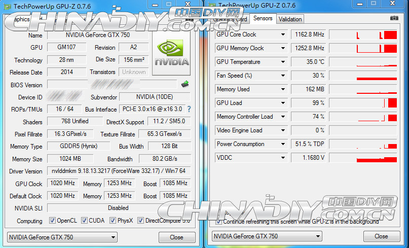
Here are the first pictures of a partner-branded GeForce GTX 750 graphics card taken apart. It reveals a couple of things - to begin with, the GM107 silicon will bring about some genuine performance per Watt improvements, despite being based on the existing 28 nm silicon fab process, and second, that cards based on the chip will be extremely cheap to build, giving NVIDIA a good chance to strengthen its position in the sub-$200 market segment. This particular card is cooled by a simple fan-heatsink that's essentially a chunk of metal with a fan latched on to it. The card relies on a simple 2+1 phase VRM, which draws power from a single 6-pin PCIe power connector. NVIDIA is expected to launch the GTX 750 and GTX 750 Ti a little later this month.
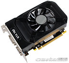
Source: ChinaDIY
Add your own comment

54 Comments on GTX 750 Taken Apart, Sips Power from a Single 6-pin Connector

#1
darkangel0504
How I hate this PCB, so ugly. Where are the long PCBs ?
Posted on Reply
#2
RCoon
darkangel0504How I hate this PCB, so ugly. Where are the long PCBs ?
Waste of copper for a little extra real estate. Plus it helps these cards to fit into HTPC's with limited card length :) Though I do agree small cards look ugly.
Posted on Reply
#3
zsolt_93
If it was single slot it would have looked great. Dual slot cooling makes it look ugly and thick. And 6pin on the non TI one?
Posted on Reply
#4
john_
The fact that needs a 6 pin power connector eliminates most expectations about a super efficient maxwell architecture. There was a leaked preview that was saying about no 6pin power connector in either card, 750 and 750Ti. It seems that that was a false preview, a lie, maybe a paid article to create a little more hype about Maxwell.
I just lost almost all interest about Maxwell.
Posted on Reply
#5
rokazs1
john_The fact that needs a 6 pin power connector eliminates most expectations about a super efficient maxwell architecture. There was a leaked preview that was saying about no 6pin power connector in either card, 750 and 750Ti. It seems that that was a false preview, a lie, maybe a paid article to create a little more hype about Maxwell.
I just lost almost all interest about Maxwell.
My thoughts exactly
Posted on Reply
#6
thebluebumblebee
Sub $200? SUB $200!!!! Really? (go take a look at the GTS 450, or GT 640, (no 6 pin connector) or GTX 650 and what price those were at) Video cards are WAY over priced these days. Look at how simple the card is. If this comes out for more than $130, I'll throw a fit. :p I realize that time marches on, that the technology and performance increases, and that inflation happens (and the devaluing of the dollar), but today we have single GPU's selling for >$700. Go back to the HD 5870 when it was introduced, when it was top dog, and see how much it was going for.
zsolt_93If it was single slot it would have looked great. Dual slot cooling makes it look ugly and thick. And 6pin on the non TI one?
Single slot=noisy. Or are they trying to make it look more impressive?
Posted on Reply
#7
MxPhenom 216
ASIC Engineer
john_The fact that needs a 6 pin power connector eliminates most expectations about a super efficient maxwell architecture. There was a leaked preview that was saying about no 6pin power connector in either card, 750 and 750Ti. It seems that that was a false preview, a lie, maybe a paid article to create a little more hype about Maxwell.
I just lost almost all interest about Maxwell.
Why because it doesn't consume 20w like you were hoping, and built up unrealistic expectations from reading "RUMORED" articles?
Posted on Reply
#8
awesomesauce
I dream about 2-3-4 GM107 silicon on one single PCB :clap:
Posted on Reply
#9
john_
MxPhenom 216Why because it doesn't consume 20w like you were hoping, and built up unrealistic expectations from reading "RUMORED" articles?
I was expecting 15W to tell you the truth.
Posted on Reply
#10
Crap Daddy
What if reference will not need a 6 pin? What if it has 640 SP?
Posted on Reply
#11
matar
Nvidia give us back the high Shader clocks not that 65Mhz extra funny boost clocks
that's why a Fermi With a 384 cores easily beats a 768 cores on the kepler because each core on the Fermi has 2x computing power of the kepler . thanks to the shader clocks.
I Prefer performance over efficiency.
Posted on Reply
#12
HumanSmoke
Crap DaddyWhat if reference will not need a 6 pin? What if it has 640 SP?
Exactly my understanding of the situation.
john_The fact that needs a 6 pin power connector eliminates most expectations about a super efficient maxwell architecture. There was a leaked preview that was saying about no 6pin power connector in either card, 750 and 750Ti. It seems that that was a false preview, a lie, maybe a paid article to create a little more hype about Maxwell.
The other side of that coin could be some non-reference SKUs will be fitted with a 6-pin connector (and likely some OTT proprietary cooler and oversized shroud) while the reference version will not...and for some reason, some people are pushing the PCI-E 6-pin as a design specification rather than an option.
Posted on Reply
#13
john_
HumanSmokeThe other side of that coin could be some non-reference SKUs will be fitted with a 6-pin connector (and likely some OTT proprietary cooler and oversized shroud) while the reference version will not...and for some reason, some people are pushing the PCI-E 6-pin as a design specification rather than an option.
It could be, but even if it really needs the extra power connector we will have to wait to see how much close will be to 75 Watts. A 750 NON Ti with 768 cores at, for example, 85W, is really good, it is just not as good as this was saying
NVIDIA GM107 "Maxwell" Silicon Pictured | techPowerUp


A little info about price, if of course this end up correct.
Felbukkantak az érkező GTX 750 Ti modellek, jön a Radeon R9 280 és R7 265 | Tech2.hu
It looks like a price tag for 750Ti between 650Ti boost(before going EOL) and GTX660 if I am not mistaken(the prices exclude VAT).
Posted on Reply
#14
Devon68
Not to sound like a AMD fanboy but I just read about the rumored AMD R9 265 which looks better than this (specs/price weise) but nothing is certain.
Posted on Reply
#15
HumanSmoke
john_. A 750 NON Ti with 768 cores at, for example, 85W, is really good, it is just not as good as this was saying
Two points:
1. If you're estimate that the 750 non-Ti eats 85W, how do you explain the Asus card not needing auxiliary power?
The naked PCB (from my earlier post that I linked to- and which seems to have been ignored)

The retail package

and,
2. I think it has been established that GK107 is 640 core/ 5 SMX / 128 core per SMX (information also noted in my earlier post, and publicized >>here<<)
Posted on Reply
#16
WithoutWeakness
For those complaining about the power consumption, remember that this is still on a 28nm node. Maxwell is likely only slightly more efficient than Kepler and the rumored low power consumption of cards is probably due to the expected 20nm process that most of the chips will be built on. Intel's Ivy Bridge brought the power consumption of desktop i5/i7 chips down from 95W to 77W compared to Sandy Bridge (23% reduction) but it needed a drop from 32nm to 22nm to do so. I wouldn't at all be surprised if we see the 750 and 750Ti show up later on with 20nm chips and no added PCIe power connectors as they would easily be the fastest cards on the market powered by the PCIe slot alone.
Posted on Reply
#17
zsolt_93
So you try to tell us that it will be worse than the gtx650/650ti both in performance and probably power too? Then why not just rebrand and profit? I still trust Wizzard over your claims from other websites that this is not a 640SP part. That would be a huge flop, lower shader count and less performance for the Ti, the other doesn't really matter as the regular GTX650 is junk. I can tolerate the 6pin on overclocked boards, or just for cleaner power and less strain on the pcie power delivery, as every PSU nowadays has at least one plug. I am sure that some manufecturers like the Asus above opt for cost saving. That PCB looks even more horrible than the one in the OP, it has place for much more components that are just left out to save money, and the 6pin location is damn awkvard, yet they will ask the same price and claim that it is an OC version.
Well.. 2 weeks or so till the (at least paper) launch. It will all become clear then.
Posted on Reply
#18
Arjai
Look at the cute little puppy! cooome here booiy!

Good puppy good boy...:rolleyes:
Posted on Reply
#19
john_
HumanSmokeTwo points:
1. If you're estimate that the 750 non-Ti eats 85W, how do you explain the Asus card not needing auxiliary power?
The naked PCB (from my earlier post that I linked to- and which seems to have been ignored)

The retail package

and,
2. I think it has been established that GK107 is 640 core/ 5 SMX / 128 core per SMX (information also noted in my earlier post, and publicized >>here<<)
1. I don't. It is just a hypothesis, nothing more.
I have seen that picture and the strange thing about this PCB is the upper left corner where someone can see something that looks like a 6 pin connector. An early engineering sample maybe with a strangely positioned power connector?

2. Established? Not really considering that all over the place specs where talking about a 768 cores 750 and a 960 cores 750Ti, WITH gpu-z screenshots. So, those screenshots where wrong? Then it seems that whatever we knew about these cards yesterday, it is false today.

With "only" 512 cores on 750, 75W isn't really something strange. 650 with 384 cores was a 64W card. A 512 cores card with a new optimized design a couple of years latter needing less or about 75W is just something normal I think. 750Ti with "only" 640 cores I could guess it will end up close to 90W?

I personally still guessing here, nothing more. Info about these cards changes rapidly day after day.
Posted on Reply
#21
Crap Daddy
I still trust Wizzard over your claims from other websites that this is not a 640SP part. That would be a huge flop.
I haven't seen anywhere W1zz saying something about this card. On the other hand this is the successor of Kepler GK107, a part with 384SP which was used in the GTX650, a low performance desktop part but rather successful in the mobile variants. For the 650 Ti Nvidia used the GK106 which is a different beast altogether, fully enabled sporting 960 CC (768 for the 650Ti) and having more than twice as much power consumption and twice as fast as the GTX650. Now look at all these leaks and tell me what do you think about GM107? Compare with GK107 almost double SP, probably almost same power consumption, maybe 75% faster on the same 28nm. Ain't life sweet? Except Nvidia uses a cut down version for the 750 (one SMX disabled) and the full chip for the Ti so we won't see this huge performance increase (remember that the 650 Ti has a GK106).
Posted on Reply
#22
HumanSmoke
john_I have seen that picture and the strange thing about this PCB is the upper left corner where someone can see something that looks like a 6 pin connector. An early engineering sample maybe with a strangely positioned power connector?
Well, the Asus card pictured in the second image tends to lean towards the card being retail rather than "an early engineering sample", and the solder points for the optional 6-pin auxiliary power are clearly visible....I would have thought.
Posted on Reply
#23
Xzibit
They also said
VideoCardz.comGigabyte GTX 750 OC (GV-N750OC-1GI) is a 512 CUDA cores Maxwell graphics card. Some GTX 750 models are not equipped with power connectors, but since we are looking at factory-overclocked model, it does have one 6-pin power plug. The difference between GM107-400 and GM107-300 lays in the number of CUDAs and TMUs. The difference between GTX 750 Ti and GTX 750 is also in memory size. The GTX 750 has only 1GB by default. The rest is pretty much the same, although the clocks are slightly different — all GTX 750s have 400 MHz slower memory (5 GHz).


The ASUS 750 is OC model but does not need a 6pin but the Gigabyte does. Just adds to the confusion.

The PCB from OP looks more inline with the Gigabyte and not the ASUS one.


None look like the Asus.
Posted on Reply
#24
john_
HumanSmokeWell, the Asus card pictured in the second image tends to lean towards the card being retail rather than "an early engineering sample", and the solder points for the optional 6-pin auxiliary power are clearly visible....I would have thought.
I haven't really seen the ASUS picture carefully. When you are used to see a specific connector in a specific place you don't usually consider something totally different that also doesn't look logical to end up in a retail card. You think that this is just a unique case, an engineering part where strange positioning of stuff and sometimes wires are more common.
Posted on Reply
#25
alwayssts
Devon68Not to sound like a AMD fanboy but I just read about the rumored AMD R9 265 which looks better than this (specs/price weise) but nothing is certain.
Whomever designed Pitcairn deserves a medal...gotta wonder how much of their profit over the last 2 years came from that chip. I bet it is a huge, huge chunk.

Not too tough to estimate a rough guess, though.

Scary math ahead.

(5400*128)/8 = 86.4gbps (bandwidth)
86.4/56.25 = 1.536TF (max usable shader compute)
1.536TF/960*2 = 800mhz
1150 (boost clock)/800*.16666 (special function) = ~.24
1.24*800 = 992mhz
992*960 = 1.9TF
1.9TF/(1024*2) = 930mhz (265 clockspeed is probably '925mhz' from amd, 975 AIB like 270)
1.9*56.25 = 107gbps
107*8/256 = 3348mhz (using 930mhz)
4800/3348 = 1.433
.433*.16 = ~6-7%

Obviously that number changes a little when considering slight efficiency differences (like tex units, which could bring it down a few percent), use cases (compute would be closer to the raw difference), and the core clock could be a little slower to a quite a bit faster than 930mhz, which while when faster increases performance more linearly than bw, would throw the difference bw makes off as obviously it would require more.

Yeah, it'll be faster at stock...but pretty close while being a much larger chip (even if salvage and using cheap 5ghz ram). That said, more logic + ideally low clocks (~900mhz/<5000mhz, where the process and mem controller are aimed) should keep power in check. The fact amd sells cheap and (usually) nvidia overcharges should keep the prices pretty close. It really comes down to two things:

1. How high can the mem clock on GM107, because while special function/bw voodoo of 16-17% will help at a higher clock when bw is scarce, it will be equally disproportionate scaling if bandwidth cannot feed the shaders.

2. How high can the core scale on 265? If limited to (for example) 1050mhz like 270, and the memory is crap elpida and hits (perhaps) 5300mhz, and the gm107 uses 6ghz on it's superior memory controller reaching closer to 7ghz overclocked, in theory around 1200mhz (little less on both counts) they could be roughly equal. How that plays out in power consumption considering die size, ram amount, etc is a good question.

Would that outcome surprise anyone? I bet it would not...two pretty similar-performing parts overall, even if massively different.
Posted on Reply
Add your own comment
Apr 24th, 2024 10:25 EDT change timezone

New Forum Posts

Popular Reviews

Controversial News Posts