Tuesday, January 27th 2015

GTX 970 Memory Drama: Plot Thickens, NVIDIA has to Revise Specs
It looks like NVIDIA's first response to the GeForce GTX 970 memory allocation controversy clearly came from engineers who were pulled out of their weekend plans, and hence was too ambiguously technical (even for us). It's only on Monday that NVIDIA PR swung into action, offering a more user-friendly explanation on what the GTX 970 issue is, and how exactly did they carve the GM204 up, when creating the card.
According to an Anandtech report, which cites that easy explanation from NVIDIA, the company was not truthful about specs of GTX 970, at launch. For example, the non-public document NVIDIA gave out to reviewers (which gives them detailed tech-specs), had clearly mentioned ROP count of the GTX 970 to be 64. Reviewers used that count in their reviews. TechPowerUp GPU-Z shows ROP count as reported by the driver, but it has no way of telling just how many of those "enabled" ROPs are "active." The media reviewing the card were hence led to believe that the GTX 970 was carved out by simply disabling three out of sixteen streaming multiprocessors (SMMs), the basic indivisible subunits of the GM204 chip, with no mention of other components like the ROP count, and L2 cache amount being changed from the GTX 980 (a full-fledged implementation of this silicon).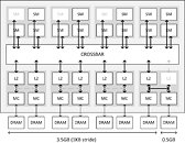
 NVIDIA explained to Anandtech that there was a communication-gap between the engineers (the people who designed the GTX 970 ASIC), and the technical marketing team (the people who write the Reviewer's Guide document, and draw the block-diagram). This team was unaware that with "Maxwell," you could segment components previously thought indivisible, or that you could "partial disable" components.
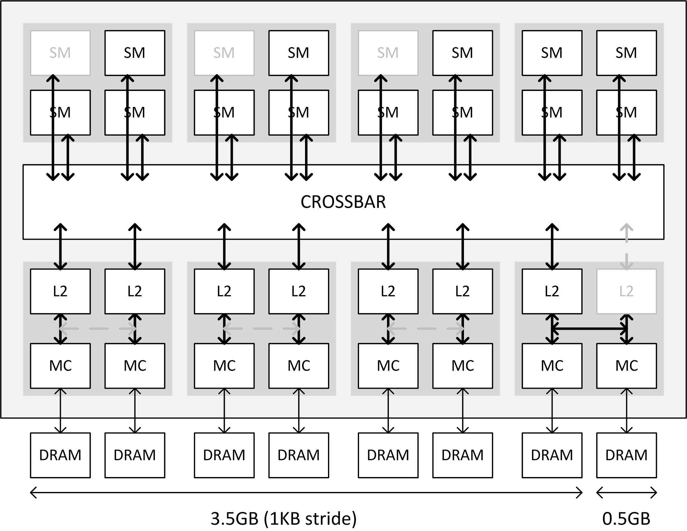
It turns out that in addition to three SMX units being disabled (resulting in 1,664 CUDA cores), NVIDIA reduced the L2 cache (last-level cache) on this chip to 1.75 MB, down from 2 MB, and also disabled a few ROPs. The ROP count is effectively 56, and not 64. The last 8 ROPs aren't "disabled." They're active, but not used, because their connection to the crossbar is too slow (we'll get to that in a bit). The L2 cache is a key component of the "crossbar." Think of the crossbar as a town-square for the GPU, where the various components of the GPU talk to each other by leaving and picking-up data labeled with "from" and "to" addresses. The crossbar routes data between the four Graphics Processing Clusters (GPCs), and the eight memory controllers of 64-bit bus width each (which together make up its 256-bit wide memory interface), and is cushioned by the L2 cache.
The L2 cache itself is segmented, and isn't a monolithic slab of SRAM. Each of the eight memory controllers on the GM204 is ideally tied to its segment of the L2 cache. Also tied to these segments are segments of ROPs. With NVIDIA reducing the L2 cache amount by disabling one such segment. Its component memory controller is instead rerouted to the cache segment of a neighbouring memory controller. Access to the crossbar for that memory controller is hence slower. To make sure there are no issues caused to the interleaving of these memory controllers, adding up to the big memory amount figure that the driver can address, NVIDIA partitioned the 4 GB of memory to two segments. The first is 3.5 GB large, and is made up of memory controllers with access to their own segments of the L2; the second segment is 512 MB in size, and is tied to that memory controller which is rerouted.
The way this partitioning works, is that the 3.5 GB partition can't be read while the 512 MB one is being read. Only to an app that's actively using the entire 4 GB of memory, there will be a drop in performance, because the two segments aren't being read at the same time. The GPU is either addressing the 3.5 GB segment, or the 512 MB one. Hence, there's a drop in performance to be expected, again, for apps that use up the entire 4 GB of memory.
While it's technically correct that the GTX 970 has a 256-bit wide memory interface, and given its 7.00 GHz (GDDR5-effective) memory clock, that translates to 224 GB/s of bandwidth on paper, not all of that memory is uniformly fast. You have 3.5 GB of it having normal access to the crossbar (the town-square of the GPU), and 512 MB of it having slower access. Therefore, the 3.5 GB segment really just has 196 GB/s of memory bandwidth (7.00 GHz x 7 ways to reach the crossbar x 32-bit width per chip), which can be said with certainty. Nor can we say how this segment affects the performance of the memory controller whose crossbar port it's using, if the card is using its full 4 GB. We can't tell how fast the 512 MB second segment really is. But it's impossible for the second segment to make up 28 GB/s (of the 224 GB/s), since NVIDIA itself claims this segment is running slower. Therefore NVIDIA's claims of GTX 970 memory bandwidth being 224 GB/s at reference clocks is inaccurate.
Why NVIDIA chose to reduce cache size and ROP count will remain a mystery. We can't imagine that the people designing the chip will not have sufficiently communicated this to the driver and technical marketing teams. To claim that technical marketing didn't get this the first time around, seems like a hard-sell. We're pretty sure that NVIDIA engineers read reviews, and if they saw "64 ROPs" on a first-page table, they would have reported it up the food-chain at NVIDIA. An explanation about this hardware change should have taken up an entire page in the technical documents the first time around, and NVIDIA could have saved itself a lot of explanation, much of it through the press.
Source:
Anandtech
According to an Anandtech report, which cites that easy explanation from NVIDIA, the company was not truthful about specs of GTX 970, at launch. For example, the non-public document NVIDIA gave out to reviewers (which gives them detailed tech-specs), had clearly mentioned ROP count of the GTX 970 to be 64. Reviewers used that count in their reviews. TechPowerUp GPU-Z shows ROP count as reported by the driver, but it has no way of telling just how many of those "enabled" ROPs are "active." The media reviewing the card were hence led to believe that the GTX 970 was carved out by simply disabling three out of sixteen streaming multiprocessors (SMMs), the basic indivisible subunits of the GM204 chip, with no mention of other components like the ROP count, and L2 cache amount being changed from the GTX 980 (a full-fledged implementation of this silicon).

It turns out that in addition to three SMX units being disabled (resulting in 1,664 CUDA cores), NVIDIA reduced the L2 cache (last-level cache) on this chip to 1.75 MB, down from 2 MB, and also disabled a few ROPs. The ROP count is effectively 56, and not 64. The last 8 ROPs aren't "disabled." They're active, but not used, because their connection to the crossbar is too slow (we'll get to that in a bit). The L2 cache is a key component of the "crossbar." Think of the crossbar as a town-square for the GPU, where the various components of the GPU talk to each other by leaving and picking-up data labeled with "from" and "to" addresses. The crossbar routes data between the four Graphics Processing Clusters (GPCs), and the eight memory controllers of 64-bit bus width each (which together make up its 256-bit wide memory interface), and is cushioned by the L2 cache.
The L2 cache itself is segmented, and isn't a monolithic slab of SRAM. Each of the eight memory controllers on the GM204 is ideally tied to its segment of the L2 cache. Also tied to these segments are segments of ROPs. With NVIDIA reducing the L2 cache amount by disabling one such segment. Its component memory controller is instead rerouted to the cache segment of a neighbouring memory controller. Access to the crossbar for that memory controller is hence slower. To make sure there are no issues caused to the interleaving of these memory controllers, adding up to the big memory amount figure that the driver can address, NVIDIA partitioned the 4 GB of memory to two segments. The first is 3.5 GB large, and is made up of memory controllers with access to their own segments of the L2; the second segment is 512 MB in size, and is tied to that memory controller which is rerouted.
The way this partitioning works, is that the 3.5 GB partition can't be read while the 512 MB one is being read. Only to an app that's actively using the entire 4 GB of memory, there will be a drop in performance, because the two segments aren't being read at the same time. The GPU is either addressing the 3.5 GB segment, or the 512 MB one. Hence, there's a drop in performance to be expected, again, for apps that use up the entire 4 GB of memory.
While it's technically correct that the GTX 970 has a 256-bit wide memory interface, and given its 7.00 GHz (GDDR5-effective) memory clock, that translates to 224 GB/s of bandwidth on paper, not all of that memory is uniformly fast. You have 3.5 GB of it having normal access to the crossbar (the town-square of the GPU), and 512 MB of it having slower access. Therefore, the 3.5 GB segment really just has 196 GB/s of memory bandwidth (7.00 GHz x 7 ways to reach the crossbar x 32-bit width per chip), which can be said with certainty. Nor can we say how this segment affects the performance of the memory controller whose crossbar port it's using, if the card is using its full 4 GB. We can't tell how fast the 512 MB second segment really is. But it's impossible for the second segment to make up 28 GB/s (of the 224 GB/s), since NVIDIA itself claims this segment is running slower. Therefore NVIDIA's claims of GTX 970 memory bandwidth being 224 GB/s at reference clocks is inaccurate.
Why NVIDIA chose to reduce cache size and ROP count will remain a mystery. We can't imagine that the people designing the chip will not have sufficiently communicated this to the driver and technical marketing teams. To claim that technical marketing didn't get this the first time around, seems like a hard-sell. We're pretty sure that NVIDIA engineers read reviews, and if they saw "64 ROPs" on a first-page table, they would have reported it up the food-chain at NVIDIA. An explanation about this hardware change should have taken up an entire page in the technical documents the first time around, and NVIDIA could have saved itself a lot of explanation, much of it through the press.
138 Comments on GTX 970 Memory Drama: Plot Thickens, NVIDIA has to Revise Specs
When I said AMD was less competitive recently, it was more from a power efficiency and cost point of view. Performance wise 290X is only marginally worse than 980, but because of the poor efficiency and higher manufacturering cost (~ 20% larger die size) the 290X has to be sold with a far smaller margin than 980.
I fully expect the new 380X to be faster than 980. However what's more important for AMD is to find a way to bring the die size (cost) and power consumption down to a level which is closer or better than the Maxwells. If not, then eventually the new flagship will be again priced as a mid-range product once 980Ti is out and that's not good for the profit margin.
never saw that coming...
KitGuru - Nvidia slammed with class-action lawsuit over GeForce GTX 970 specifications
IncGamers - Nvidia faces lawsuit over GTX 970 specification claims
You can read the lawsuit at Scribd here.
[Source]
on that note are we to believe that a new specially developed option(linked IMC port(optional post bin)) put into a chips design specifically to up yields and create more profit(or less scraped parts essentially)
within a new generation arch, was Not talked about in presentation's to the company's own staff, way before release etc,,
, very very feckin dubious,,, all of it reek's of incompetence or fraud (via the see no evil pact) either way I would never buy anything on a whim from nvidia again, and i was going to (ie 69$ tegra 3 7'' pad, Was going to be mine) ill look elsewhere first now as will a few others.
Still setting the bar pretty low if an "enthusiast" sites knowledge base is deemed acceptable because it rivals that of a marketing/PR Dept.:p There's a actually a low-cost solution staring everyone in the face. Why not just give those affected a R9 290 or 290X? AMD's board partners(many of whom sell Nvidia cards) have AMD inventory backlogthanks to the channel stuffing Rory instituted. With AMD's designs not exactly flying of the shelves, why not cut a deal? :pHappy shopping. The only thing at this stage with a Tegra inside that interests me is an Audi.
Look at the "post" from 28 january. I don't know what to think, is the guy full of shit or not?