Monday, October 26th 2015
GDDR5X Puts Up a Fight Against HBM, AMD and NVIDIA Mulling Implementations
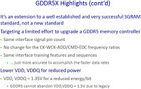
There's still a little bit of fight left in the GDDR5 ecosystem against the faster and more energy-efficient HBM standard, which has a vast and unexplored performance growth curve. The new GDDR5X standard offers double the bandwidth per-pin compared to current generation GDDR5, without any major design or electrical changes, letting GPU makers make a seamless and cost-effective transition to it.
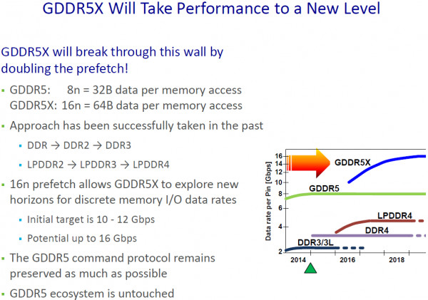
In a presentation by a DRAM maker leaked to the web, GDDR5X is touted as offering double the data-rate per memory access, at 64 byte/access, compared to 32 byte/access by today's fastest GDDR5 standard, which is currently saturating its clock/voltage curve at 7 Gbps. GDDR5X breathes a new lease of live to the ageing DRAM standard, offering 10-12 Gbps initially, with a goal of 16 Gbps in the long term. GDDR5X chips will have identical pin layouts to their predecessors, and hence it should cost GPU makers barely any R&D to implement them.
 When mass-produced by companies like Micron, GDDR5X is touted to be extremely cost-effective compared to upcoming HBM standards, such as HBM2. According to a Golem.de report, both AMD and NVIDIA are mulling GPUs that support GDDR5X, so it's likely that the two could reserve expensive HBM2 solutions for only their most premium GPUs, and implement GDDR5X on their mainstream/performance solutions, to keep costs competitive.
Source:
Golem.de
In a presentation by a DRAM maker leaked to the web, GDDR5X is touted as offering double the data-rate per memory access, at 64 byte/access, compared to 32 byte/access by today's fastest GDDR5 standard, which is currently saturating its clock/voltage curve at 7 Gbps. GDDR5X breathes a new lease of live to the ageing DRAM standard, offering 10-12 Gbps initially, with a goal of 16 Gbps in the long term. GDDR5X chips will have identical pin layouts to their predecessors, and hence it should cost GPU makers barely any R&D to implement them.


69 Comments on GDDR5X Puts Up a Fight Against HBM, AMD and NVIDIA Mulling Implementations
As to the 10 and 15 percent, I made an error. I switched the 15% savings and 10% final size in my mind, before typing. You've managed to go from 3.75%, to 10%, to 15% without ever acknowledging your mistake. I may have flipped the numbers once, but you managed to have a nearly 500% change without ever even stopping to evaluate your own words.
On top of this, you tell me you're not interested in conjecture, then level the Pascal conjecture. I'm feeling as though this is trolling.
Finally, have you read the link you're citing? I ask, because you and I seem to have issues getting the same understanding. The interposer is functionally a slab of conductive traces. Assuming that the HBM and GDDR5 memory controllers are functionally interchangeable electrically with only minor changes (I've seen nothing that indicates this not to be reasonable, as HBM is not a functionally new type of storage), the memory controller gets to be shrunk down because all of the interconnects just jump off the silicon wherever possible. There's no need to design the traces such that they run to the outside of the package (or the underside with BGA), which is part of the reason why I'm assuming that the die space is conserved (it isn't reasonably a function of HBM needing less memory to control -per your linked article-, and definitely not a function of less interconnection -again, per your article the interface is much wider-). Under this interpretation, the memory controller traces, a necessary part of the memory controller, are offloaded to the interposer. The interposer therefore is critical to the memory controller, but isn't powered because it's just a myriad of conductive paths. If your interpretation of what I said was that the memory controller was divided onto the interposer and GPU die then we are at odds here. What I mean to say, in less accurate terms, is that AMD bought space on the GPU die by adding enough extra wiring dangling out of the GPU (read: the interposer).
I'll quote Joe Macri (AMD employee in charge of HBM) again:
By this diagram, you can see that the interposer is merely full of electrical pathways. The logic die in the HBM stack is what you are thinking about for saving on die space, NOT the interposer.
You've got the package substrate, which is the PCB. You've got a GPU die with just the interconnection points shown. Connect them, using your diagram. What the picture shows is that the interposer can take any placement on the GPU, and run conductors three dimensionaly to the DRAM dies. This means no matter what the GPU traces look like, it can connect to the DRAM. I'm assuming, given how obvious this statement is, that we can agree to it.
Now back to intelligent people land. What packages do chips come in? There's BGA, which is more expensive because it requires a PCB with multiple layers. Those are a royal PITA. There's packaging that places all of the pins on the outside edge. Those are great for manufacturing, but the trade off is that the inside of the GPU has to accomodate traces getting to those pins. Conductors are threaded through the system, such that space is wasted on the die for easy access to the pins.
AMD is demonstrating BGA, where there is no need for multi-layer PCBs. They've basically taken that difficulty out of the equation by having an interposer do it. The interposer can be produced relatively cheaply if it uses older lithography, but it's far easier to make that layering traces inside of fiberglass.
So at this point, I need you to be reasonable. Looking at the picture above how do you connect the GPU to the DRAM? You can argue that a 7+ layer PCB would work, or you can argue that the memory controller has been given free reign to reach for the DRAM chips like an octopus. I'll be blunt, if you can find a way to make 7+ layer PCBs consistently and cheaply I'll give the argument to you. In my experience 3 layers is enough of a nightmare.
AMD isn't insanely stupid. They add cost by making an interposer. They decrease costs (or improve performance) by decreasing necessary silicon on the more expensive GPU die by having interconnect spaghetti throughout the interposer. I don't care about the logic die. Unless you can prove otherwise, my understanding is that it is basically just a secondary controller similar to what we already enmebbed into our current DRAM chips. I haven't seen anything to indicate that isn't the case, but more specifically this article never indicates otherwise. Their exact words are:
"Although the interposer is essential, the truly intriguing innovation in the HBM setup is the stacked memory. Each HBM memory stack consists of five chips: four storage dies above a single logic die that controls them."
I'm even going out on a limb here, and calling out your other statement. Here it is:In your own article, they explain exactly why your assertion that the interposer may not be needed for HBM is crap. Here's the quote:
"Macri explained that the interposer is completely passive; it has no active transistors because it serves only as an electrical interconnect path between the primary logic chip and the DRAM stacks.
The interposer is what makes HBM's closer integration between DRAM and the GPU possible. A traditional organic chip package sits below the interposer, as it does with most any GPU, but that package only has to transfer data for PCI Express, display outputs, and some low-frequency interfaces. All high-speed communication between the GPU and memory happens across the interposer instead."
I'm just a schmuck, who you can choose to ignore. The problem is that when your expert says the exact opposite, he's no longer an expert somehow? You really should stop arguing here. Your pictures prove my points. Your articles prove the points. It requires a very narrow and difficult to justify perspective in order to claim what you've said. They clearly say that the interposer is offloading high speed communication that used to be on the GPU. They clearly diagram said high speed communication is between the GPU and DRAM. I don't know how else you want to try and justify that the interposer isn't largely an extension of the memory controller.
In my mind the only argument that remains is that they didn't outright say that the interposer is an extension of the memory controller. The catch is that they can't. The high speed interconnects of the memory controller are in the interposer (they confirmed this), as well as the power feeds and interconnects to the rest of the PCB. As such, it's a device which performs multiple functions of which some are usually on the PCB. If you'd like to understand why that is, let's review exactly how carefully Macri chose the words that were utilized:
"When I asked Macri about this issue, he expressed confidence in AMD's ability to work around this capacity constraint. In fact, he said that current GPUs aren't terribly efficient with their memory capacity simply because GDDR5's architecture required ever-larger memory capacities in order to extract more bandwidth. As a result, AMD "never bothered to put a single engineer on using frame buffer memory better," because memory capacities kept growing. Essentially, that capacity was free, while engineers were not. Macri classified the utilization of memory capacity in current Radeon operation as "exceedingly poor" and said the "amount of data that gets touched sitting in there is embarrassing.""
This is why Macri said that 4 GB on Fiji wouldn't be an issue. He said they had "a couple of engineers" on it, and that simply throwing more RAM at the problem was always the solution. What Macri said here is tantamount to "we don't ever optimize," yet he's said it in a way that the interviewer bought as a valid explanation for why they needed to optimize now. Talk about getting punched in the gut, then asking "please sir, may I have another?" Whatever else can be said, Macri is aware that the interposer is vital for memory access. He acquiesces that memory usage has historically been crap.
After all of that, you're still arguing that AMD hasn't chosen to make gains by introducing cheap processes to save on the expensive ones? You can't see where a 65 nm interposer saving them from a couple million dollars in engineering work isn't necessary? I'm sorry, but I just can't put it more simply than that. Heck, Macri himself said that high speed data was the primary purpose of the interposer. If memory access isn't high speed data, when PCI-e was cited as low speed, I haven't the slightest clue what is.
The rest of it... I dunno how you get that from what I wrote... I didn't have any hidden meanings or ideas. :P
GDDR5X If price wise is pretty close same price as current GDDR5 then it could be used on say lower end of the high end cards, for example use current products gtx960/970, HBM will be limited to 980 and up.
cadaveca stated that "PASCAL cards shown already have a rather normal-looking GPU substrate". Every picture of Pascal shown publicly is based off of that mock up. Are you telling me that, like cadaveca, you believe Pascal has HBM2 but will require no interposer to connect it electrically to the GPU?
I'm fully aware that Pascal has taped out and TSMC has already fabbed a hot lot for test and verification - I was part of that article discussion. It just doesn't have any direct relevance to the matter we are discussing here.
Not too sure what the problem is TBH. I don't think anyone is expecting GDDR5/GDDR5X to be the memory of choice for enthusiast graphics cards going forward, and the reference PCBs for the GTX 950/960/970, R9 370/380 aren't exactly behemoths.
If you are talking maunufacturing cost, well that's not exactly staggering. An 8-layer certified/coloured/silk screened lead-free PCB of 8" length costs around $2 more per unit than a 6" one in a worst case scenario.
And how little has the GPU length changed between GDDR3 and GDDR5? That doubled the density. Yet a 3850 is roughly the same length as almost any GPU you listed.
Both Nvidia's and AMD's next generation of enthusiast-level GPUs are slated for HBM2 use, so why prattle on about the 980 Ti ?
Wide I/O memory technologies are undoubtedly the way of the future, especially since with an active interposer you could incorporate not just processor and memory, but auxilliary chips (bridge chips, I/O, voltage, secondary co-processors such as ARM processors for example). But that technology - at a price that can be absorbed by mainstream parts is still some way off. If it were viable now, AMD would surely have designed a second-tier GPU (Fiji is effectively Tonga doubled in any case) for use with HBM. The technology is still not mature enough, and the cost penalty too high.
The only way you could make that determination is if you know what profit (or loss) margin AMD sell the card at in relation to a similarly priced card with GDDR5?
Do you?
I'm guessing you don't.
Considering the assets of sapphire technology (AMD's #1 PCB manuf) have grown 323% year over year and their cash on hand has gone up 42.9k% I would say they are probably making a decent amount per card.
source
If you are going to quote company finances at me, at least get the right company.
Sapphire Tech - y'know, the one that actually makes AMD cards - is basically swimming in red ink. The only bright revenue stream at the moment comes from being a supplier to Apple.
And BTW, Sapphire isn't AMD's #1 PCB manufacturer, PC Partner (Sapphire's parent company) is.
PC Partner are also the parent company of the Nvidia-based brands Zotac, Manli, Inno3D, and Leadtek. PC Partner also manufacture cards (in addition to AMD reference) for Point of View, PNY (along with Palit), Zogis, and ELSA - all Nvidia-based.
Let's put it this way I want HBM. Fuck GDDR5x and its long ass cards.