Tuesday, April 12th 2016

NVIDIA "Pascal" GP100 Silicon Detailed

The upcoming "Pascal" GPU architecture from NVIDIA is shaping up to be a pixel-crunching monstrosity. Introduced as more of a number-cruncher in its Tesla P100 unveil at GTC 2016, we got our hands on the block diagram of the "GP100" silicon which drives it. To begin with, the GP100 is a multi-chip module, much like AMD's "Fiji," consisting of a large GPU die, four memory-stacks, and silicon wafer (interposer) acting as substrate for the GPU and memory stacks, letting NVIDIA drive microscopic wires between the two. The GP100 features a 4096-bit wide HBM2 memory interface, with typical memory bandwidths of up to 1 TB/s. On the P100, the memory ticks at 720 GB/s.

At its most top-level hierarchy, the GP100 is structured much like other NVIDIA GPUs, with the exception of two key interfaces - bus and memory. A PCI-Express gen 3.0 x16 host interface connects the GPU to your system, the GigaThread Engine distributes workload between six graphics processing clusters (GPCs). Eight memory controllers make up the 4096-bit wide HBM2 memory interface, and a new "High-speed Hub" component, wires out four NVLink ports. At this point it's not known if each port has a throughput of 80 GB/s (per-direction), or all four ports put together.
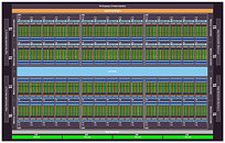
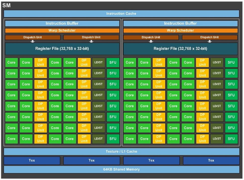
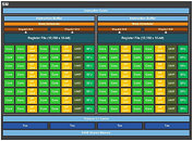
The GP100 features six graphics processing clusters (GPCs). These are highly independent subdivisions of the GPU, with their own render front and back-ends. With the "Pascal" architecture, at least with the way it's implemented on the GP100, each GPC features 10 streaming multiprocessors (SMs), the basic number crunching machinery of the GPU. Each SM holds 64 CUDA cores. The GPC hence holds a total of 640 CUDA cores, and the entire GP100 chip holds 3,840 CUDA cores. Other vital specs include 240 TMUs. On the Tesla P100, NVIDIA enabled just 56 of the 60 streaming multiprocessors, working out to a CUDA core count of 3,584.

The "Pascal" architecture appears to facilitate very high clock speeds. The Tesla P100, despite being an enterprise part, features a core clock speed as high as 1328 MHz, with GPU Boost frequency of 1480 MHz, and a TDP of 300W. This might scare you, but you have to take into account that the memory stacks have been moved to the GPU package, and so the heatsink interfacing with it all, will have to cope with the combined thermal loads of the GPU die, the memory stacks, and whatever else makes heat on the multi-chip module.

Lastly, there's the concept of NVLink. This interconnect developed in-house by NVIDIA makes multi-GPU setups work much like a modern multi-socket CPU machine, in which QPI (Intel) or HyperTransport (AMD) links provide super-highways between neighboring sockets. Each NVLink path offers a bandwidth of up to 80 GB/s (per direction), enabling true memory virtualization between multiple GPUs. This could prove useful for GPU-accelerated HPC systems, in which one GPU has to access memory controlled by a neighboring GPU, while the software sees the sum of the two GPUs' memory as one unified and contiguous block. The Pascal Unified Memory system lets advanced GPU programming models like CUDA 8 oversubscribe memory beyond what the GPU physically controls, and up to the system memory.
Add your own comment

50 Comments on NVIDIA "Pascal" GP100 Silicon Detailed

#26
Vayra86
So, the consumer Geforce GP100 has

- No HBM2 (GDDR5X)
- No NVlink (no functionality on x86, no point otherwise)
- A lower enabled SM count (they will never start with the maximum GP100 can offer, they still need a later release top-end 'ti' version, which means we will see at least two SM's disabled, or more, unless they get really good yields - which is highly unlikely given the maturity of 14/16nm)
- Probably similar or slightly bumped clocks

Also, about positioning of cards, first version GP100 will have a much greater gap with the later version with all SM enabled because the difference will be at least 2 SM's. Nvidia will have a big performance jump up its sleeve, totally different from how they handled things with Kepler and 780ti.
Posted on Reply
#27
acperience7
With all the bandwidth in a PCIe 3.0 X16 slot why is not possible to use that in place of NVLink? They are no where near saturated with modern cards from the testing I have seen.
Posted on Reply
#28
Tsukiyomi91
With the consumer grade chips coming in a few months' time, I will wait for TPU to get their hands on some samples before I consider upgrading.
Posted on Reply
#29
bug
jabbadapWell yeah there's no x86 processor which have nvlink support(and I don't believe there ever will be such a processor). But GPU-to-GPU link should be possible with x86 processor, thus dual gpu cards could use it between gpus and use pcie to communicate with cpu(GTC 2016 nvlink graph).
Physically, were would you send the NVLink data if the card is only connected to a PCIe slot?
Posted on Reply
#30
arbiter
FordGT90ConceptThis doesn't sound like much/any improvement on the async shaders front. It also only represents an increase of 16.7% in CUDA core count compared to Titan X. I think I'm disappointed.
Typical AMD fanboy being an idiot when talking about a card that doesn't have a single use for async shaders to start with. go back to your mom's basement. Tesla cards don't need it for the work they do which is NOT gaming.
Vayra86So, the consumer Geforce GP100 has

- No HBM2 (GDDR5X)
- No NVlink (no functionality on x86, no point otherwise)
- A lower enabled SM count (they will never start with the maximum GP100 can offer, they still need a later release top-end 'ti' version, which means we will see at least two SM's disabled, or more, unless they get really good yields - which is highly unlikely given the maturity of 14/16nm)
- Probably similar or slightly bumped clocks

Also, about positioning of cards, first version GP100 will have a much greater gap with the later version with all SM enabled because the difference will be at least 2 SM's. Nvidia will have a big performance jump up its sleeve, totally different from how they handled things with Kepler and 780ti.
Nvlink isn't needed on consumer end at this time. As for HBM don't know what high end cards will have but mid range will be gddr5. Speculating and making claims based on just making up stupid crap only makes said person look an idiot. If high end x80 cards are based on GP100/P100 chips they should be HBM2 since that will be controller on them.
Posted on Reply
#31
efikkan
FordGT90ConceptThis doesn't sound like much/any improvement on the async shaders front.
Do you have access to detailed information about the internal GPU scheduling?
Stop spinning the myth that Nvidia doesn't support async compute, it's a planned feature of CUDA 8 scheduled for June.
FordGT90ConceptIt also only represents an increase of 16.7% in CUDA core count compared to Titan X. I think I'm disappointed.
P100 increased the FP32 performance by 73% over Titan X, 88% over 980 Ti, using only 17% more CUDA cores. That's a pretty impressive increase in IPC.

Game performance doesn't scale linearly with FP32, but we should be able to get 50-60% higher gaming performance on a such chip.
The Quim ReaperWho cares....GP100 cards are still nearly a year away.

Wake me up a week before launch.
We wouldn't see any GP100 based graphics cards anytime soon, GP102 will be the fastest one in a graphics card this year.
acperience7With all the bandwidth in a PCIe 3.0 X16 slot why is not possible to use that in place of NVLink? They are no where near saturated with modern cards from the testing I have seen.
NVLink is designed for compute workloads, no graphic workload needs it.
Posted on Reply
#32
ManofGod
Well, thank you for the information. Now we will still have to wait and see what end up being released and how fast it will truly be. (Or not be.)
Posted on Reply
#33
FordGT90Concept
"I go fast!1!11!1!"
arbiterTypical AMD fanboy being an idiot when talking about a card that doesn't have a single use for async shaders to start with. go back to your mom's basement. Tesla cards don't need it for the work they do which is NOT gaming.
You're right, async shaders are useless in Tesla because graphics and compute don't intermingle. That said, FirePro cards still have ACEs to handle async compute workloads for compatibility sake--NVIDIA should too.
efikkanDo you have access to detailed information about the internal GPU scheduling?
Stop spinning the myth that Nvidia doesn't support async compute, it's a planned feature of CUDA 8 scheduled for June.
Unless there's major changes in the GigaThread Engine, there's nothing on the diagram that suggests it is fixed.
efikkanP100 increased the FP32 performance by 73% over Titan X, 88% over 980 Ti, using only 17% more CUDA cores. That's a pretty impressive increase in IPC.
You're right, it is baring in mind that Tesla is designed specifically for FP32 and FP64 performance. We'll have to wait and see if that translates to graphics cards.
Posted on Reply
#34
the54thvoid
Intoxicated Moderator
We'll all wait and see what comes from Pascal. For my part, I think I'll be keeping my Maxwell till 2017. I think Vega and the consumer GP100 equivalent will be my next options.
As for the whole Async shambles, its not going to be Nvidia's downfall. If people think that's a reality, you need to ease off the red powder you're snorting.
Most likely outcome is very simply Pascal using brute power to deliver the experience.
I don't mind which way it goes, I just hope it goes one way to force the other side to go cheaper.
Posted on Reply
#35
HumanSmoke
FordGT90ConceptYou're right, async shaders are useless in Tesla because graphics and compute don't intermingle. That said, FirePro cards still have ACEs to handle async compute workloads for compatibility sake--NVIDIA should too.
FirePro's have ACE's because a FirePro is literally a Radeon bundled with an OpenCL driver. The only real differences aren't at the GPU level (aside from possibly binning) - they are memory capacity and PCB/power input layout. Nvidia began the bifurcation of its GPU line with theGK210, a revision of GK110 aimed solely at compute workloads, and a GPU that never saw the light of day as a consumer grade card. GP100 looks very much like the same design ethos.
FordGT90ConceptYou're right, it is baring in mind that Tesla is designed specifically for FP32 and FP64 performance. We'll have to wait and see if that translates to graphics cards.
A big selling point for GP100 is its mixed compute ability, which includes FP16 for deep learning neural networks.
FordGT90ConceptUnless there's major changes in the GigaThread Engine, there's nothing on the diagram that suggests it is fixed.
Difficult to make any definitive comment based on a single HPC orientated part, but my understanding is Nvidia is leaving most of the architectural reworking until Volta (which apparently will have compatibility with Pascal hardware interfaces for HPC). Nvidia will rely on more refined preemption (this Pascal overview is one of the better around), better perf/watt due to the lower ALU to SM ratio, and a fast ramp of first-gen 16nm product at the expense of a time consuming architecture revision. Whether the brute force increase in GPU power, the perf/$, and Perf/watt offset any deficiencies in async compute in comparison to AMD will have to wait until we see the products, but I'm guessing that since AMD themselves are hyping perf/watt rather than all out performance, I really don't expect any major leaps from AMD either. Just as apropos, is whether AMD have incorporated conservative rasterization into Polaris.
the54thvoidAs for the whole Async shambles, its not going to be Nvidia's downfall.
True enough. The difference in performance is marginal for the most part with people reduced to quoting percentages because the actual frames per second differences sound too trivial. It's great that AMD's products get an uplift using the DX12 code path using async compute, but I can't help but feel that the general dog's breakfast that is DX12 and its driver implementations at present tend to reduce the numbers to academic interest - mores o given that the poster boy for async compute- AotS - seems to be a game people are staying away from in droves.
the54thvoidMost likely outcome is very simply Pascal using brute power to deliver the experience.
Agreed. Nvidia seem to have targeted time to market and decided on a modest increase in GPU horsepower across their three most successful segments (if SweClockers is to be believed), while AMD seem content to mostly replace their more expensive to produce and less energy efficient GPUs - something long overdue in the discrete mobile market.
the54thvoidI don't mind which way it goes, I just hope it goes one way to force the other side to go cheaper.
Hopefully....but the cynic in me thinks that Nvidia and AMD might just continue their unspoken partnership in dovetailing price/product.
Posted on Reply
#36
FordGT90Concept
"I go fast!1!11!1!"
HumanSmokeDifficult to make any definitive comment based on a single HPC orientated part, but my understanding is Nvidia is leaving most of the architectural reworking until Volta (which apparently will have compatibility with Pascal hardware interfaces for HPC). Nvidia will rely on more refined preemption (this Pascal overview is one of the better around), better perf/watt due to the lower ALU to SM ratio, and a fast ramp of first-gen 16nm product at the expense of a time consuming architecture revision. Whether the brute force increase in GPU power, the perf/$, and Perf/watt offset any deficiencies in async compute in comparison to AMD will have to wait until we see the products, but I'm guessing that since AMD themselves are hyping perf/watt rather than all out performance, I really don't expect any major leaps from AMD either. Just as apropos, is whether AMD have incorporated conservative rasterization into Polaris.
That's what I was afraid of...hence my disappointment. :( Pascal appears to be an incremental update, not a major update; Polaris too for that matter. If Polaris doesn't have conservative rasterization, add that to my disappointment list. :laugh:

I think both AMD and NVIDIA are banking on higher IPC + higher clocks. If NVIDIA can manage 1.3 GHz clocks on TSMC where AMD can only manage 800-1000 MHz at GloFo, AMD is going to lose the performance competition; this may be why they're touting performance/watt, not performance. :(
Posted on Reply
#37
HumanSmoke
Ferrum MasterUnless they use it in dual cards instead of the PLX bridge or some laptop setups... most probably the block will be ommited in consumer cards.
Could be an interesting option to retain a single NVLink for dual GPU cards - a bit overkill on the bandwidth front, but it would make the overall bill of materials fractionally lower not having to pay Avago for the lane extender chips I suppose.
bugIt was officially announced NVLink only works with POWER CPUs at this time. So no, it's not for home use.
Really? Wasn't that pretty much dispelled with the announcement of the dual Xeon E5 DGX-1 andQuanta's x86 support announcement during their DGX-1 demonstration? SuperMicro has also announced x86 NVLink compatibility in a semi-leaked form. Nvidia also announced NVLink compatibility for ARM64 architectures during the same GTC presentation
Vayra86So, the consumer Geforce GP100 has
- No HBM2 (GDDR5X)
- No NVlink (no functionality on x86, no point otherwise)
- A lower enabled SM count (they will never start with the maximum GP100 can offer, they still need a later release top-end 'ti' version, which means we will see at least two SM's disabled, or more, unless they get really good yields - which is highly unlikely given the maturity of 14/16nm)
- Probably similar or slightly bumped clocks
That seems like a lot of supposition being related as fact with no actual proof. Historically, GeForce parts have higher clocks than HPC parts, and Nvidia has amortized production costs by leading with salvage parts - so these are very possible, but I've just provided evidence of x86 NVLink support, and I haven't seen any indication that GP100 won't be paired with HBM2. Where did you see this supposed fact?
Posted on Reply
#38
Vayra86
HumanSmokeThat seems like a lot of supposition being related as fact with no actual proof. Historically, GeForce parts have higher clocks than HPC parts, and Nvidia has amortized production costs by leading with salvage parts - so these are very possible, but I've just provided evidence of x86 NVLink support, and I haven't seen any indication that GP100 won't be paired with HBM2. Where did you see this supposed fact?
I know, it was just something I pulled out as my assumption of what it may look like. Facts, not at all :) About HBM2, we will have to see, apart from the memory controller being set on the current part I am having trouble justifying it in terms of being 'required' when GDDR5X is available. Nvidia will want to cut corners if they can, and they have ample time to alter the design, though Im not sure its economically smart to do so.
Posted on Reply
#39
Xzibit
HumanSmokeCould be an interesting option to retain a single NVLink for dual GPU cards - a bit overkill on the bandwidth front, but it would make the overall bill of materials fractionally lower not having to pay Avago for the lane extender chips I suppose.

Really? Wasn't that pretty much dispelled with the announcement of the dual Xeon E5 DGX-1 andQuanta's x86 support announcement during their DGX-1 demonstration? SuperMicro has also announced x86 NVLink compatibility in a semi-leaked form. Nvidia also announced NVLink compatibility for ARM64 architectures during the same GTC presentation


That seems like a lot of supposition being related as fact with no actual proof. Historically, GeForce parts have higher clocks than HPC parts, and Nvidia has amortized production costs by leading with salvage parts - so these are very possible, but I've just provided evidence of x86 NVLink support, and I haven't seen any indication that GP100 won't be paired with HBM2. Where did you see this supposed fact?
1. QuantaPlex T21W-3U:
This x86 server employs high-bandwidth and energy-efficient NVLink interconnects to enable extremely fast communication between eight of the latest NVidia GPU modules (SXM2).
x86 still use PCIe Swith between GPU & CPU. I think only IBM with newest Power CPU will be able to do NVLink GPU-to-CPU
Posted on Reply
#40
HumanSmoke
Xzibitx86 still use PCIe Swith between GPU & CPU. I think only IBM with newest Power CPU will be able to do NVLink GPU-to-CPU
The original contention put forward by bug was that NVLink could not be used as a bridge between GPUs in a dual GPU card as put forward by Ferrum Master. That is incorrect, as is your assumption that we were talking about GPU<->CPU traffic.


FWIW, the advantages ofGPU point to point bandwidth advances using NVLink have been doing the rounds for the best part of a week since the Quanta and SuperMicro info dropped.
Posted on Reply
#41
Ferrum Master
HumanSmokeCould be an interesting option to retain a single NVLink for dual GPU cards - a bit overkill on the bandwidth front
If latency is low enough it should render possible to address neighboring GPU's RAM pool without a performance tax... That's the best thing that could happen. So I suppose overkill on the bandwidth front is really not possible ;).
Posted on Reply
#42
bug
HumanSmokeThe original contention put forward by bug was that NVLink could not be used as a bridge between GPUs in a dual GPU card as put forward by Ferrum Master. That is incorrect, as is your assumption that we were talking about GPU<->CPU traffic.


FWIW, the advantages ofGPU point to point bandwidth advances using NVLink have been doing the rounds for the best part of a week since the Quanta and SuperMicro info dropped.
But what's the physical medium NVLink uses on a x86 platform? I haven't seen any "SLI bridge"-style thing and the card is only connected to a PCIe bus.

Edit: You seem too eager to take marketing slides as actual real-world gains.
Posted on Reply
#43
Ferrum Master
bugBut what's the physical medium NVLink uses on a x86 platform? I haven't seen any "SLI bridge"-style thing and the card is only connected to a PCIe bus.

Edit: You seem too eager to take marketing slides as actual real-world gains.
SERVERS! If the server cluster will use x86, they will use a demux bridge to nvlink! It is really simple as that... They have no conventional connectors there, it is all custom made, they could make their own boards as shown per slides.
Posted on Reply
#44
Aquinus
Resident Wat-man
btarunrAt this point it's not known if each port has a throughput of 80 GB/s (per-direction), or all four ports put together.
This article seems to indicate that a single NVLink connection is rated for 20GB/s, not 80GB. The total theoretical aggregate bandwidth appears to be 80GB but, that appears to be highly variable depending on how much data is being set at any given time. That is, full bandwidth isn't realized unless each message is packed as full as it can get and the smaller each "packet" (I'm thinking network/PCI-E like mechanics here,) is, the worse bandwidth is going to get. So don't plan on sending a ton of small messages over NVLink, it seems to like large ones. The situation would have to be pretty special to realize a full 80GB/s and even still, if the following article is to be trusted, even in the best of circumstances, no more than 70GB/s will probably get realized due to overhead introduced with smaller sized data and that assumes load can be equally spread out accross NVLink connections. I would rather see PCI-E v4.
www.hardware.fr/news/14587/gtc-tesla-p100-debits-pcie-nvlink-mesures.html
Posted on Reply
#45
bug
Ferrum MasterSERVERS! If the server cluster will use x86, they will use a demux bridge to nvlink! It is really simple as that... They have no conventional connectors there, it is all custom made, they could make their own boards as shown per slides.
My point exactly. x86 won't be able to use NVLink. Instead, custom designs will.
Posted on Reply
#46
efikkan
FordGT90ConceptUnless there's major changes in the GigaThread Engine, there's nothing on the diagram that suggests it is fixed.
You still need to prove that it's broken. Async shaders is a feature of Maxwell, and is a planned feature of CUDA 8. Nvidia even applied for patents on the technology several years back.

People constantly needs to be reminded that async shaders is an optional feature of Direct3D 12, and Nvidia so far has prioritized implementing it for CUDA as there really still are no good games on the market to utilize it anyway.
Posted on Reply
#47
FordGT90Concept
"I go fast!1!11!1!"
Async shaders have been implemented since D3D11 (not "optional"). AMD implemented them as they should be in GCN; NVIDIA half-assed it making the entire GPC have to be scheduled for compute or graphics, not both (not Microsoft's intended design). There are plenty of resources on the internet that show it is broke going all of the way back to Kepler (which should have had it because it was a D3D11 card). Game developers haven't been using it likely because it causes a framerate drop on NVIDIA cards. Async shading is getting the most traction on consoles (especially PlayStation 4) because they're trying to squeeze every drop of performance they can out of the console.

"...Nvidia so far has prioritized implementing it for CUDA..." and that's the problem! Async shaders are a feature of graphics pipeline, not CUDA. CUDA 8 makes no mention of it, nor should it.

Edit: Here's the article: ext3h.makegames.de/DX12_Compute.html
MakeGames.deCompute and 3D engine can not be active at the same time as they utilize a single function unit.
The Hyper-Q interface used for CUDA is in fact supporting concurrent execution, but it's not compatible with the DX12 API.
If it was used, there would be a hardware limit of 32 asynchronous compute queues in addition to the 3D engine.
MakeGames.de
  • The workload on a single queue should always be sufficient to fully utilize the GPU.

    There is no parallelism between the 3D and the compute engine so you should not try to split workload between regular draw calls and compute commands arbitrarily. Make sure to always properly batch both draw calls and compute commands.

    Pay close attention not to stall the GPU with solitary compute jobs limited by texture sample rate, memory latency or anything alike. Other queues can't become active as long as such a command is running.
  • Compute commands should not be scheduled on the 3D queue.

    Doing so will hurt the performance measurably. The 3D engine does not only enforce sequential execution, but the reconfiguration of the SMM units will impair performance even further.

    Consider the use of a draw call with a proxy geometry instead when batching and offloading is not an option for you. This will still save you a few microseconds as opposed to interleaving a compute command.
  • Make 3D and compute sections long enough.

    Switching between compute and 3D queues results in a full flush of all pipelines. The GPU should have spent enough time in one mode to justify the penalty for switching.

    Beware that there is no active preemption, a long running shader in either engine will stall the transition.
If developers start implementing async shaders into their games, they'll always be nerfed on Maxwell and older cards. Backwards compatibility support will be poor because NVIDIA didn't properly implement the feature going into D3D11.
Posted on Reply
#48
BiggieShady
FordGT90ConceptUnless there's major changes in the GigaThread Engine, there's nothing on the diagram that suggests it is fixed.
This article mentions something in that vein, specifically Pascal's ability to preempt threads on instruction boundaries rather than waiting for end of a draw call ... www.theregister.co.uk/2016/04/06/nvidia_gtc_2016/
Posted on Reply
#49
Xzibit
BiggieShadyThis article mentions something in that vein, specifically Pascal's ability to preempt threads on instruction boundaries rather than waiting for end of a draw call ... www.theregister.co.uk/2016/04/06/nvidia_gtc_2016/
They are referring to Compute Preemption.

If you recall

Oculus Employees: “Preemption for context switches is best on AMD, Nvidia possibly catastrophic”

They might have improved it. Although The WoZ was dizzy after a few minutes.
Posted on Reply
Add your own comment
May 7th, 2024 11:16 EDT change timezone

New Forum Posts

Popular Reviews

Controversial News Posts