Thursday, March 21st 2019

Samsung Develops Industry's First 3rd-generation 10nm-Class DRAM
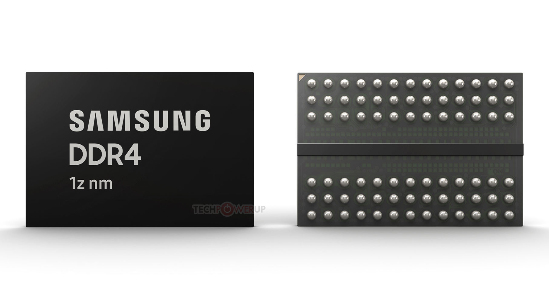
Samsung Electronics Co., Ltd., the world leader in advanced memory technology, today announced that it has developed a 3rd-generation 10-nanometer-class (1z-nm) eight-gigabit (Gb) Double Data Rate 4 (DDR4) DRAM for the first time in the industry. In just 16 months since it began mass producing the 2nd-generation 10nm-class (1y-nm) 8Gb DDR4, development of 1z-nm 8Gb DDR4 without the use of Extreme Ultra-Violet (EUV) processing has pushed the limits of DRAM scaling even further.
As 1z-nm becomes the industry's smallest memory process node, Samsung is now primed to respond to increasing market demands with its new DDR4 DRAM that has more than 20-percent higher manufacturing productivity compared to the previous 1y-nm version. Mass production of the 1z-nm 8Gb DDR4 will begin within the second half of this year to accommodate next-generation enterprise servers and high-end PCs expected to be launched in 2020.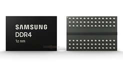 "Our commitment to break through the biggest challenges in technology has always driven us toward greater innovation. We are pleased to have laid the groundwork again for stable production of next-generation DRAM that ensures the highest performance and energy efficiency," said Jung-bae Lee, executive vice president of DRAM product & technology, Samsung Electronics. "As we build out our 1z-nm DRAM lineup, Samsung is aiming to support its global customers in their deployment of cutting-edge systems and enabling proliferation of the premium memory market."
Samsung's development of the 1z-nm DRAM paves the way for an accelerated global IT transition to next-generation DRAM interfaces such as DDR5, LPDDR5 and GDDR6 that will power a wave of future digital innovation. Subsequent 1z-nm products with higher capacities and performance will allow Samsung to strengthen its business competitiveness and solidify its leadership in the premium DRAM market for applications that include servers, graphics and mobile devices.
Following a full validation with a CPU manufacturer for eight-gigabyte (GB) DDR4 modules, Samsung will be actively collaborating with global customers to deliver an array of upcoming memory solutions.
In line with current industry needs, Samsung plans to increase the portion of its main memory production at its Pyeongtaek site, while working with its global IT clients to meet the rising demand for state-of-the-art DRAM products.
As 1z-nm becomes the industry's smallest memory process node, Samsung is now primed to respond to increasing market demands with its new DDR4 DRAM that has more than 20-percent higher manufacturing productivity compared to the previous 1y-nm version. Mass production of the 1z-nm 8Gb DDR4 will begin within the second half of this year to accommodate next-generation enterprise servers and high-end PCs expected to be launched in 2020.
Samsung's development of the 1z-nm DRAM paves the way for an accelerated global IT transition to next-generation DRAM interfaces such as DDR5, LPDDR5 and GDDR6 that will power a wave of future digital innovation. Subsequent 1z-nm products with higher capacities and performance will allow Samsung to strengthen its business competitiveness and solidify its leadership in the premium DRAM market for applications that include servers, graphics and mobile devices.
Following a full validation with a CPU manufacturer for eight-gigabyte (GB) DDR4 modules, Samsung will be actively collaborating with global customers to deliver an array of upcoming memory solutions.
In line with current industry needs, Samsung plans to increase the portion of its main memory production at its Pyeongtaek site, while working with its global IT clients to meet the rising demand for state-of-the-art DRAM products.
12 Comments on Samsung Develops Industry's First 3rd-generation 10nm-Class DRAM
But at least there's this strong push towards making more dense memory (Optane, higher modules etc). So consumers can benefit as well.
Yields and litography are deeply technical terms.
You need clean financial variables to analyze situation and control the company.
Do we know what improvements can we expect beyond 20% extra manufacturing productivity - lower power, higher density, greater speeds?
More importantly: why would Samsung tell you? It's their trade secret. :-)
Profit, Profit, Profit.