Thursday, January 28th 2021

Apple Patents Multi-Level Hybrid Memory Subsystem

Apple has today patented a new approach to how it uses memory in the System-on-Chip (SoC) subsystem. With the announcement of the M1 processor, Apple has switched away from the traditional Intel-supplied chips and transitioned into a fully custom SoC design called Apple Silicon. The new designs have to integrate every component like the Arm CPU and a custom GPU. Both of these processors need good memory access, and Apple has figured out a solution to the problem of having both the CPU and the GPU accessing the same pool of memory. The so-called UMA (unified memory access) represents a bottleneck because both processors share the bandwidth and the total memory capacity, which would leave one processor starving in some scenarios.

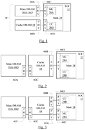
Apple has patented a design that aims to solve this problem by combining high-bandwidth cache DRAM as well as high-capacity main DRAM. "With two types of DRAM forming the memory system, one of which may be optimized for bandwidth and the other of which may be optimized for capacity, the goals of bandwidth increase and capacity increase may both be realized, in some embodiments," says the patent, " to implement energy efficiency improvements, which may provide a highly energy-efficient memory solution that is also high performance and high bandwidth." The patent got filed way back in 2016 and it means that we could start seeing this technology in the future Apple Silicon designs, following the M1 chip.

Update 21:14 UTC: We have been reached out by Mr. Kerry Creeron, an attorney with the firm of Banner & Witcoff, who provided us with additional insights about the patent. Mr. Creeron has provided us with his personal commentary about it, and you can find Mr. Creeron's quote below.

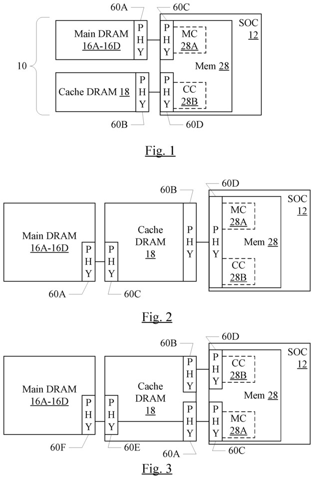
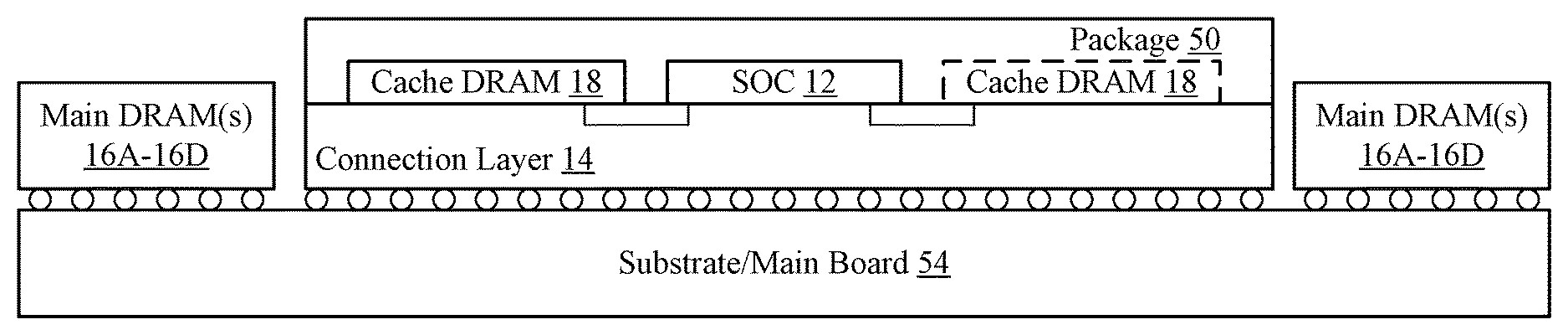
Kerry Creeron—an attorney with the firm of Banner & Witcoff.High-level, the patent covers a memory system having a cache DRAM and that is coupled to a main DRAM. The cache DRAM is less dense and has lower energy consumption than the main DRAM. The cache DRAM may also have higher performance. A variety of different layouts are illustrated for connecting the main and cache DRAM ICs, e.g. in FIGS. 8-13. One interesting layout involves through silicon vias (TSVs) that pass through a stack of main DRAM memory chips.

Theoretically, such layouts might be useful for adding additional slower DRAM to Apple's M1 chip architecture.

Finally, I note that the lead inventor, Biswas, was with PA Semi before Apple Acquired it.
Source: Apple Patent
Add your own comment

41 Comments on Apple Patents Multi-Level Hybrid Memory Subsystem

#1
TheLostSwede
News Editor
I thought the M1 already did something like this.
Posted on Reply
#2
AleksandarK
News Editor
TheLostSwedeI thought the M1 already did something like this.
Currently, the M1 has a UMA for both CPU and GPU.
Posted on Reply
#3
Vya Domus
Broadwell had basically the same thing, except the DRAM was integrated on the chip. I am not sure how worth it is to have it on the same package instead. Not every good if you're trying to save power either vs having it integrated.

So it seems to me like this is just a worse version of what Intel did with their L4 cache.
Posted on Reply
#4
bug
So... Apple just invented cached RAM access?
Posted on Reply
#5
zlobby
bugSo... Apple just invented cached RAM access?
Yes, and don't forget they invented the optimal radii of the corners of their phones.
Posted on Reply
#6
Fouquin
Vya DomusBroadwell had basically the same thing, except the DRAM was integrated on the chip. I am not sure how worth it is to have it on the same package instead. Not every good if you're trying to save power either vs having it integrated.

So it seems to me like this is just a worse version of what Intel did with their L4 cache.
Haswell and Broadwell eDRAM L4 was also its own die wired through the substrate. They did this to reduce manufacturing complexity and offer two zones of clock control for performance binning. External tiers of cache are nothing new, neither is stacked caches. This is something that goes back decades. What is new is the order of cache access, landing size, wire latency and bandwidth.

Posted on Reply
#7
Post Nut Clairvoyance
FouquinHaswell and Broadwell eDRAM L4 was also its own die wired through the substrate. They did this to reduce manufacturing complexity and offer two zones of clock control for performance binning. External tiers of cache are nothing new, neither is stacked caches. This is something that goes back decades. What is new is the order of cache access, landing size, wire latency and bandwidth.

Just wonder how it compares to EDRAM. But not expecting this to be order of magnitude faster. Should actually provide worthwhile speed boost compared to EDRAM at least, putting it on SOC die(?) instead of separate EDRAM die.
Posted on Reply
#8
TechLurker
I wonder if AMD will eventually implement similar for their own APUs, but maybe with HBM instead, or maybe even on the board again like the old Phenom-era mobo cache; except where the HBM could be used either by the CPU or the GPU as-needed.
Posted on Reply
#9
crimsontape
I wouldn't expect this to be a real performance boosting design (maybe between UMA and some wire reduced latency?), but rather a change up in the bill of materials and manufacturing approaches. This is like Intel's recent efforts in a lot of ways.

This is also in the context of Big-Small core setup. So, there may be some in-house special sauce that calls to optimizing that architecture setup against an on-package bit of DRAM.

Throw on some degree of MRAM tech or whatever to provide some quasi speedy permanent cache on the package... Really start veering off that "it's either L$, RAM or on the disk" dogma, and incorporate layers of software priority for OS and applications to help further optimize latency... That could get interesting for reducing the PCB foot print of these devices.
Posted on Reply
#10
mouacyk
Tacking on eDRAM to a fast x86 processor is one thing, but adding it to a slow ARM chip is quite another.
Posted on Reply
#11
ZoneDymo
mouacykTacking on eDRAM to a fast x86 processor is one thing, but adding it to a slow ARM chip is quite another.
but what about adding it to a fast ARM chip? like is the case here?
Posted on Reply
#12
mouacyk
ZoneDymobut what about adding it to a fast ARM chip? like is the case here?
3.2GHz core isn't exactly fast by today's standards, but what is its actual non-core speed that feeds the cache? When Apple/Intel first introduced it on Broadwell, core and uncore were running well in excess of 4GHz.
Posted on Reply
#13
zlobby
TechLurkerI wonder if AMD will eventually implement similar for their own APUs, but maybe with HBM instead, or maybe even on the board again like the old Phenom-era mobo cache; except where the HBM could be used either by the CPU or the GPU as-needed.
I'm sure it never ocurred to the engineers at AMD.
Posted on Reply
#15
InVasMani
bugSo... Apple just invented cached RAM access?
They modified what others invented marginally to avoid lawsuits and patented that as their very own cutting edge innovation that will cost a torso because a arm and leg is no longer enough. AMD should just replace the DRAM on the substrate with a FPGA and patent that. They can look into how or why to utilize it after. Hey look we did a thing do too.
Posted on Reply
#16
RJARRRPCGP
TechLurkerI wonder if AMD will eventually implement similar for their own APUs, but maybe with HBM instead, or maybe even on the board again like the old Phenom-era mobo cache; except where the HBM could be used either by the CPU or the GPU as-needed.
FTR, socket 462 was their last FSB desktop platform! AMD is well known for moving stuff to on-die, before Intel. For Intel, OTOH, they still did FSB until the first-gen Core i-series.
Posted on Reply
#17
Aquinus
Resident Wat-man
This feels like just another level in the memory hierarchy. I had always felt that the CPU needed something between the last level of on-die CPU cache and system memory. HBM seemed like it would be the best option for this kind of thing because of its memory density and fairly low power usage and the on-package memory that Apple uses seems to be a lot like that. So it makes a boatload of sense that there would be a need for something between flash memory, which is already ungodly fast, and DRAM that's further away from the CPU/GPU/NPU/XYZPU. Imagine having 16GB of "really fast" memory, but having 128GB of "still pretty fast" memory to support it? If the caching strategy is sound, performance is good, and it's as good as having 144GB of memory, then that sounds pretty damn sexy if you ask me.

With that said though, as the owner of a top of the line MacBook Pro that's expensive as a kidney, I know that Apple will absolutely make you pay through the nose for it.
SteevoSo like socket Super 7 in the late 90s that had on board cache Apple is now doing it?
The Apple G3 and G4 had an off die cache on the same package as the CPU. It's nothing new. It just makes sense to have cache closer to the actual cores using it for the sake of latency. It depends on where in the memory hierarchy you need improvement.

Edit: I mean, what does this look like? I used one of these when StarCraft was brand new. This isn't new tech. We just have better tech to use it with.
Posted on Reply
#18
mechtech
Looks like Rambus is at it again with the patents...............oh wait ;)
Posted on Reply
#19
bug
AquinusThis feels like just another level in the memory hierarchy. I had always felt that the CPU needed something between the last level of on-die CPU cache and system memory. HBM seemed like it would be the best option for this kind of thing because of its memory density and fairly low power usage and the on-package memory that Apple uses seems to be a lot like that. So it makes a boatload of sense that there would be a need for something between flash memory, which is already ungodly fast, and DRAM that's further away from the CPU/GPU/NPU/XYZPU. Imagine having 16GB of "really fast" memory, but having 128GB of "still pretty fast" memory to support it? If the caching strategy is sound, performance is good, and it's as good as having 144GB of memory, then that sounds pretty damn sexy if you ask me.

With that said though, as the owner of a top of the line MacBook Pro that's expensive as a kidney, I know that Apple will absolutely make you pay through the nose for it.
Caches need to be fast (low-latency) and they are power hungry because of that. HBM is kinda the opposite of that.
Posted on Reply
#20
Aquinus
Resident Wat-man
bugCaches need to be fast (low-latency) and they are power hungry because of that. HBM is kinda the opposite of that.
Latency gets worse the further away from the compute cores you go when it comes to the memory hierarchy. I'm not suggesting another level of external cache because SRAM is expensive and runs hot. I'm suggesting that this is adding a level to the memory hierarchy between cache and system memory. It doesn't need to have latency better than cache, just better than system memory while maintaining high bandwidth.
Posted on Reply
#21
bug
AquinusLatency gets worse the further away from the compute cores you go when it comes to the memory hierarchy. I'm not suggesting another level of external cache because SRAM is expensive and runs hot. I'm suggesting that this is adding a level to the memory hierarchy between cache and system memory. It doesn't need to have latency better than cache, just better than system memory while maintaining high bandwidth.
Of course, but I was addressing this:
HBM seemed like it would be the best option for this kind of thing because of its memory density and fairly low power usage and the on-package memory that Apple uses seems to be a lot like that.
Posted on Reply
#22
Wirko
bugCaches need to be fast (low-latency) and they are power hungry because of that. HBM is kinda the opposite of that.
Caches need to be low-latency but how does Apple's "cache DRAM" fit in here? What technology could it be based on if it's expected to offer cosiderably lower latency than the main DRAM?
Posted on Reply
#23
bug
WirkoCaches need to be low-latency but how does Apple's "cache DRAM" fit in here? What technology could it be based on if it's expected to offer cosiderably lower latency than the main DRAM?
If it's not mentioned in the patent itself, we may never know. It could be either a form of cheaper SRAM or some plain DDR that lower latency just by the virtue of being on the same die.

Edit: Lo and behold, the update says it's just DDR.
Posted on Reply
#24
Aquinus
Resident Wat-man
WirkoCaches need to be low-latency but how does Apple's "cache DRAM" fit in here? What technology could it be based on if it's expected to offer cosiderably lower latency than the main DRAM?
Remember that little thing called Crystal Well that Intel made for certain Broadwell chips; an eDRAM cache paired with the more beefy iGPUs? Think that, but with more capacity. While electricity travels pretty fast, a lot of latency is introduced by the length of the circuit. Having something like stacked DRAM really close to the CPU can offer better latency than that of DIMMs that are physically much further away. This is why I think something like HBM or stacked DRAM on the same package as the CPU could act as a level in the memory hierarchy that's between the last level of CPU cache and system memory.
Posted on Reply
#25
Ravenas
That lifestyle company can't be besting Intel... ;)
Posted on Reply
Add your own comment
May 2nd, 2024 20:31 EDT change timezone

New Forum Posts

Popular Reviews

Controversial News Posts