Monday, June 21st 2021

AMD Ryzen Embedded V3000 SoCs Based on 6nm Node, Zen 3 Microarchitecture
AMD's next generation Ryzen Embedded V3000 system-on-chips aren't simply "Cezanne" dies sitting on BGA packages, but rather based on a brand new silicon, according to Patrick Schur, a reliable source with leaks. The die will be built on the more advanced 6 nm silicon fabrication node, whilst still being based on the current "Zen 3" microarchitecture. There are several things that set it apart from the APU silicon of the current-generation, making it more relevant for the applications the Ryzen Embedded processor family is originally built for.
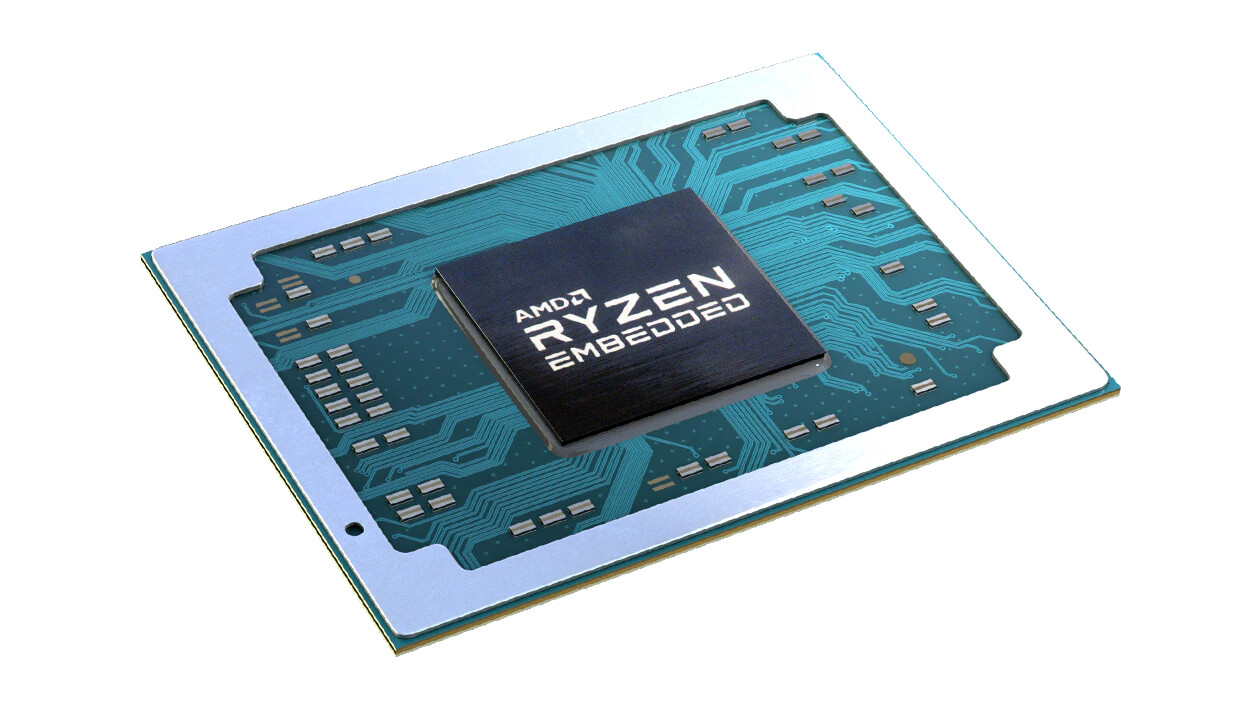
Built in the FP7r2 BGA package, the V3000 silicon features an 8-core/16-thread CPU based on the "Zen 3" microarchitecture. There are also an integrated GPU based on the RDNA2 graphics architecture, with up to 12 CUs, a dual-channel DDR5 memory interface, a 20-lane PCI-Express 4.0 root complex, with up to 8 lanes put out for PEG; two USB4 ports, and two 10 GbE PHYs. AMD could design at least three SKUs based on this silicon, spanning TDP bands of 15-30 W and 35-54 W.
Sources:
Patrick Schur (Twitter), VideoCardz
Built in the FP7r2 BGA package, the V3000 silicon features an 8-core/16-thread CPU based on the "Zen 3" microarchitecture. There are also an integrated GPU based on the RDNA2 graphics architecture, with up to 12 CUs, a dual-channel DDR5 memory interface, a 20-lane PCI-Express 4.0 root complex, with up to 8 lanes put out for PEG; two USB4 ports, and two 10 GbE PHYs. AMD could design at least three SKUs based on this silicon, spanning TDP bands of 15-30 W and 35-54 W.
11 Comments on AMD Ryzen Embedded V3000 SoCs Based on 6nm Node, Zen 3 Microarchitecture
That would be more bandwidth than a Geforce 1030. This should be good enough for light 1080 gaming and medium detail, if not more since RDNA2 GPU is more modern than Pascal. There are no rumours of Infinity cache, but still, RDNA2 could have more L1 and L2 depending on the final layout.
Can't wait to see the final bench. the desktop 5600G and 5700G already have impressive performance (for integrated graphic) with Vega and DDR4. This could be a game changer.
For Rembrandt it appears like they are doing 2 Shaders Arrays of 6 CUs each(3 DCUs) and 2mb of L2, an increase of the 1mb in the Vega iGPUs. So a decent increase in the caches.
Nothing too big of a change though.
Would be really impressive if they could do like Apple and do a shared cache with CPU and iGPU( aka SLC/System level cache for Apple, though other blocks like neural stuff also use it), even more so if they do it with their vertical cache. It would be completely revolutionary in the mobile and integrated gpu space.
But that's just a pipe dream.
I don't think we're likely to see stacked cache in mobile yet though. That would necessitate a huge amount of "structural silicon" (i.e. spacers around the cache die) considering the size of APUs compared to a CCX, and would no doubt have some detrimental effects for already thermally constrained mobile designs.
So, I think that AMD could easily add something like 8 mb as infinity cache. Yes, Apple is in 5nm, but SRAM doesn't scale as logic does, in addition they are going to 6nm anyway(and have a bigger die than Cezanne despite increased density).Probably not since they grind those dies so that they end up with the same height, plus structural silicon might even help with spreading more of the heat.
In addition, could actually reduce power consumption as the part which consumes the most is the data transmission, while processing it is cheap. If you remember Broadwell, it was pretty good in energy consumption and it could even do stuff like turn off under some circumstances.
This would really help with mobile skus. But honestly, I doubt that AMD will do it in the next 2-3 years.