Tuesday, October 19th 2021

SK hynix Announces Development of HBM3 DRAM
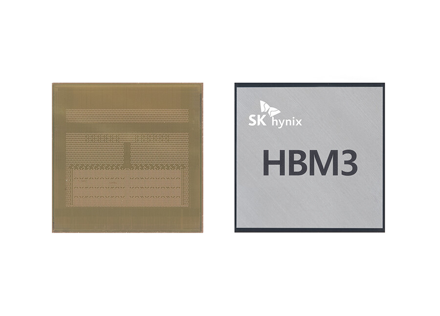
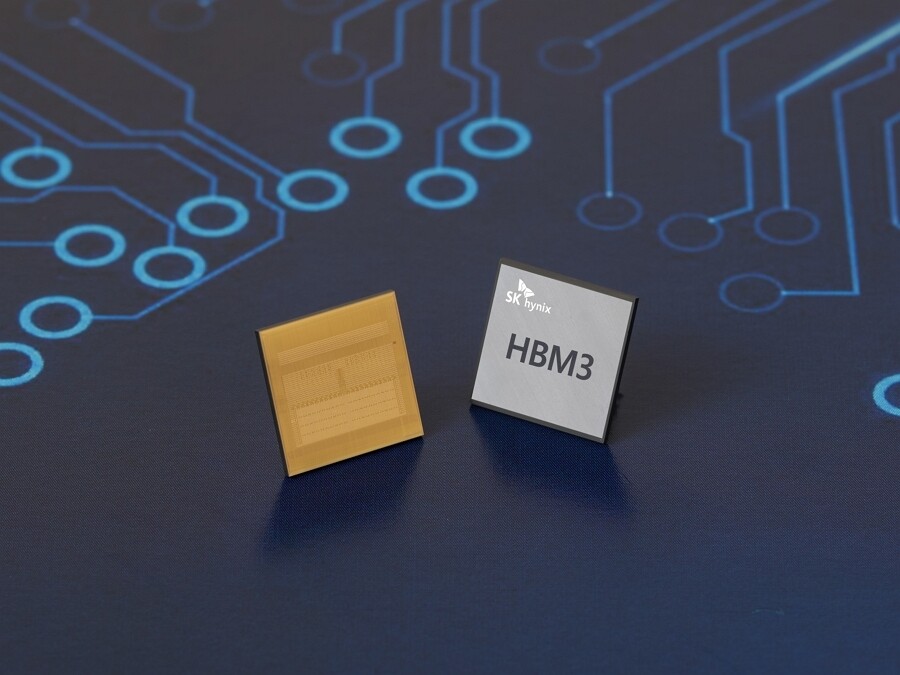
SK hynix Inc. announced that it has become the first in the industry to successfully develop the High Bandwidth Memory 3, the world's best-performing DRAM. HBM3, the fourth generation of the HBM technology with a combination of multiple DRAM chips vertically connected, is a high value product that innovatively raises the data processing rate.
The latest development, which follows the start of mass production of HBM2E in July last year, is expected to help consolidate the company's leadership in the market. SK hynix was also the first in the industry to start mass production of HBM2E. SK hynix's HBM3 is not only the fastest DRAM in the world, but also comes with the biggest capacity and significantly improved level of quality.
 The latest product can process up to 819 GB (Gigabyte) per second, meaning that 163 FHD (full-HD) movies (5 GB each) can be transmitted in a single second. This represents a 78% increase in the data-processing speed compared with the HBM2E. It also corrects data (bit) errors with the help of the built-in on-die error-correction code, significantly improving the reliability of the product.
SK hynix's HBM3 will be provided in two capacity types of 24 GB - the industry's biggest -- and 16 GB. For the 24 GB product, SK hynix engineers ground the height of a DRAM chip to approximately 30 micrometer, equivalent to a third of an A4 paper's thickness, before vertically stacking 12 chips using the through silicon via technology.
HBM3 is expected to be mainly adopted by high-performance data centers as well as machine learning platforms that enhance the level of artificial intelligence and super computing performance used to conduct climate change analysis and drug development.
"Since its launch of the world's first HBM DRAM, SK hynix has succeeded in developing the industry's first HBM3 after leading the HBM2E market," said Seon-yong Cha, Executive Vice President in charge of the DRAM development. "We will continue our efforts to solidify our leadership in the premium memory market and help boost the values of our customers by providing products that are in line with the ESG management standards."
The latest development, which follows the start of mass production of HBM2E in July last year, is expected to help consolidate the company's leadership in the market. SK hynix was also the first in the industry to start mass production of HBM2E. SK hynix's HBM3 is not only the fastest DRAM in the world, but also comes with the biggest capacity and significantly improved level of quality.
SK hynix's HBM3 will be provided in two capacity types of 24 GB - the industry's biggest -- and 16 GB. For the 24 GB product, SK hynix engineers ground the height of a DRAM chip to approximately 30 micrometer, equivalent to a third of an A4 paper's thickness, before vertically stacking 12 chips using the through silicon via technology.
HBM3 is expected to be mainly adopted by high-performance data centers as well as machine learning platforms that enhance the level of artificial intelligence and super computing performance used to conduct climate change analysis and drug development.
"Since its launch of the world's first HBM DRAM, SK hynix has succeeded in developing the industry's first HBM3 after leading the HBM2E market," said Seon-yong Cha, Executive Vice President in charge of the DRAM development. "We will continue our efforts to solidify our leadership in the premium memory market and help boost the values of our customers by providing products that are in line with the ESG management standards."
15 Comments on SK hynix Announces Development of HBM3 DRAM
Imagine a CPU fed this speed of data
NVIDIA GeForce RTX 3090 - 24 GB
Memory Bandwidth: 936 GB/secNVIDIA GeForce RTX 3080 Ti - 12 GB
Memory Bandwidth: 912 GB/secNVIDIA GeForce RTX 3080 - 10 GB
Memory Bandwidth: 760 GB/secBut the main benefits of HBM is having a lower queue latency in high bandwidth situation and lower power per bit transferred.
I had to check via Xilinx;It needs to run at 8533MHz to be close to 819GB/s.
2. 1 module = 1024 bits wide = 128 bytes wide
3. 819 GigaByte per sec = 128 Byte per Hz * __ GigaHz which gives us 819/128 GHz = 6.4 GHz
Don't take my word for it - www.anandtech.com/show/17022/sk-hynix-announces-its-first-hbm3-memory-24gb-stacks-at-up-to-64gbps
www.pcinvasion.com/amd-vega-aibs/and it would cost another $500 over where it is now. Between the high cost of HBM and the substrate costs went out of control
www.pcgamesn.com/amd-rx-vega-custom-graphics-cards
Don't take my word for it, but there are lots of mistranslations going on.
One example:While I do agree that the io is indeed "1024-bit" wide, it is for 16 channel(16 hi?) stacks which this is not.
I couldn't find a good way to distribute it over 12 layers, so it is all theoretical when it comes to the "16 channel x 64 bit" distribution. What this comes down to is, it will in practice act like a 768-bit interface.
Whenever you want to access any item, you have access 8 channels for max speed. Of course, this is a very simplistic viewpoint. In reality you will have much more than 12 items and some will be small, some large and it will have to be distributed in a complicated manner, but this is the essence of how it will work.
One more thing - you might ask why is it that GDDR6X is only 32 bit wide per memory chip and HBM is 128 bit wide per memory chip and the answer to that is 32 bit and 128 bit are the width of the connection between the memory chip and processor. It is in no way indication of what happens inside the memory chip. What is happening inside the memory chip is beyond my scope of explanation in a forum. GDDR6X is a narrow, fast connection (think 32 traffic lanes but each lane is super fast). HBM is a wider, slower connection (think 128 traffic lanes but each lane is slower).
GDDR6X - narrow 32 bit connection but very fast 21 GHz speed
HBM3 - wider 128 bit connection but slower 6.4 GHz speed
Fun fact - in 2012, AMDand Nvidia were very proud that they achieved 6 GHz speed with 256/384 bit wide bus. 10 years later, in 2022, we will have 2048/4096 bit wide bus operating at 6+ GHz.If 3080 had HBM it would be so expensive that nobody will buy it. What we need is for cards like 3070 Ti and 3080 to have 16 GB and 20 GB memory capacity. it's an atrocity that 3060 has more memory capacity than 3060 Ti, 3070, 3070 Ti and 3080. RTX 3060 has as much memory as the 3080 Ti. If you want more memory than the 3060 can provide you need to go to 3090. This is just stupid.
I'm not stupid enough to recommend 8 channel mode. Anybody can recommend HBM1 instead of 2 and 3...