Saturday, February 7th 2009

NVIDIA Designs New GTX 260 PCB, Further Reduces Manufacturing Costs
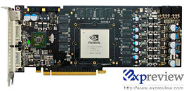
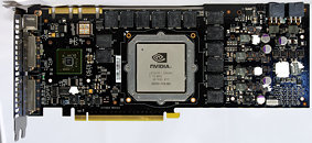
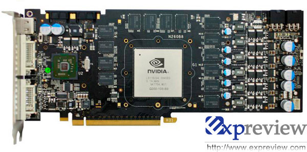
The introduction of the new G200b series graphics processors sought to revive NVIDIA's stronghold over the high-end graphics market, by reducing manufacturing costs, and facilitating high-end graphics cards at unusually low price-points, to compete with rival ATI. The first SKU using the G200b GPU was the new GeForce GTX 260. The PCB of design of the new model (P654) saw several drastic changes, that also ended up contributing to the cost-cutting: all memory chips were placed in the business end of the PCB, and the VRM area rearranged. News emerging from Expreview suggests that NVIDIA has worked out an even newer PCB reference design (model: P897) that aims mainly to cut production costs further. The reference design graphics board based on the PCB will be given the internal name "D10U-20". A short list of changes is as follows: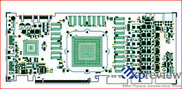
Source:
Expreview
- The number of PCB layers has been reduced from 10 to 8, perhaps to compress or remove blank, redundant or rudimentary connections
- A 4+2 phase NVVDD power design using the ADP4100 voltage regulator IC, the FBVDDQ circuit has been reduced from 2 phases to 1, and the MOSFET package has been changed from LFPAK to DPAK grouping, to reduce costs. The ADP4100 lacks the I2C interface, which means voltage control will be much more difficult than on current PCBs of the GeForce 260,280, 285 and 295
- The optional G200b support-brace has been removed
- While the length of the PCB remains the same, the height has been reduced to cut costs
- BIOS EEPROM capacity reduced from 1 Mbit (128 KB) to 512 Kb (64 KB)
- Cheaper DVI connectors


78 Comments on NVIDIA Designs New GTX 260 PCB, Further Reduces Manufacturing Costs
see video card description.
almost 12% of steam users (which is a hell of a lot of people) have the 8800 series cards. Its the most popular card overall, and almost 23% of people running DX10 hardware are doing so on an 8800 series card.
I'm pretty sure expreview just made a mistake during the translation.
that'd be around 3-4CM
at least my card does AA properly.
Its a good feature set to support well.
Unless thats removed from the hungarian versions for some reason. :)
a thinner pcb means more chance of flexing and damage .
In anycase, Galaxy uses this new design on the first gen GTX260.. really cuts the price off.
If there's no DX10 apps, how do you know if it's good o not? :roll:3Dmark Vantage IS DX10, Unigine, FarCry 2, Crysis Warhead (let's say Crysis was not, this one IS) and many other games and apps are DX10. G92 does just well on those apps, much better than the R600/RV670 in most cases, so nice try.
But with cards as powerful as the 4870's and GTX260's dropping in price, these could very well end up being next-gen mid-range cards that could make DX10+ performance better in games and maybe start to justify the costs of DX10 only games. Sure I would like to see it, but I also like the fact that you can do DX9 too if you don't have the hardware or performance capabilites for 10. And if the AMD/ATI and NV units I mentioned earlier were to become a midrange GTS350 and HD5430 or whatever have you, at an easier price point, bang for the buck would be there. Pretty much a pipe dream at this point, but the prices these cards are at now for this generation is pretty sweet. I'm curious to see how this card does, I have a feeling it will do quite well overall, there will be some that don't care if it's got less power phases or can't support voltage change via hardware, when it flat out runs like a champ. The 260 is no slouch at stock.
:toast: