 / Ryzen 5")
6
Cores
12
Threads
28 W
TDP
3.2 GHz
Frequency
4.9 GHz
Boost
Hawk Point
Codename
Socket FP7
Socket
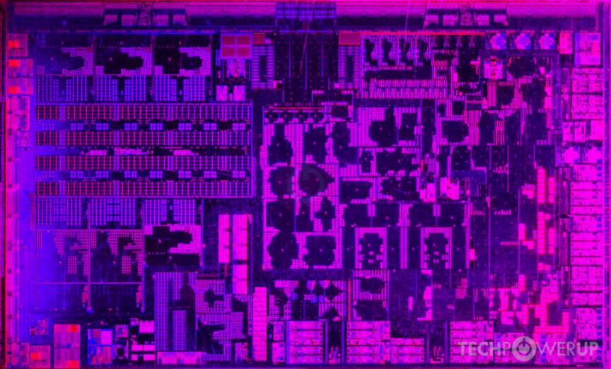
Die Shot

Connectivity
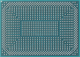
AMD Socket FP7
The AMD Ryzen 5 8540U is a mobile processor with 6 cores, launched in December 2023. It is part of the Ryzen 5 lineup, using the Zen 4 (Hawk Point) architecture with Socket FP7. Thanks to AMD Simultaneous Multithreading (SMT) the core-count is effectively doubled, to 12 threads. Ryzen 5 8540U has 16 MB of L3 cache and operates at 3.2 GHz by default, but can boost up to 4.9 GHz, depending on the workload. AMD is making the Ryzen 5 8540U on a 4 nm production node using 20,900 million transistors. The silicon die of the chip is not fabricated at AMD, but at the foundry of TSMC. The multiplier is locked on Ryzen 5 8540U, which limits its overclocking potential.
With a TDP of 28 W, the Ryzen 5 8540U consumes only little energy. AMD's processor supports DDR5 memory with a dual-channel interface. The highest officially supported memory speed is 5600 MT/s, but with overclocking (and the right memory modules) you can go even higher. For communication with other components in the system, Ryzen 5 8540U uses a PCI-Express Gen 4 connection. This processor features the Radeon 740M integrated graphics solution.
Hardware virtualization is available on the Ryzen 5 8540U, which greatly improves virtual machine performance. Programs using Advanced Vector Extensions (AVX) can run on this processor, boosting performance for calculation-heavy applications. Besides AVX, AMD has added support for the newer AVX2 and AVX-512 instructions, too.
Physical
| Socket: | AMD Socket FP7 |
|---|---|
| Foundry: | TSMC |
| Process Size: | 4 nm |
| Transistors: | 20,900 million |
| Die Size: | 137 mm² |
| Package: | FP7, FP7r2 |
| tJMax: | 100°C |
Processor
| Market: | Mobile |
|---|---|
| Production Status: | Active |
| Release Date: | Dec 6th, 2023 |
| Part#: | 100-000001326 (FP7r2) 100-000001333 (FP7) |
Performance
| Frequency: | 3.2 GHz |
|---|---|
| Turbo Clock: | up to 4.9 GHz |
| E-Core Frequency: |
3 GHz
up to 3.5 GHz |
| Base Clock: | 100 MHz |
| Multiplier: | 32.0x |
| Multiplier Unlocked: | No |
| TDP: | 28 W |
| Configurable TDP: | 15-30 W |
Architecture
| Codename: | Hawk Point |
|---|---|
| Generation: |
Ryzen 5
(Zen 4 (Hawk Point)) |
| Memory Support: | DDR5 |
| LPDDR5x Speed: | 7500 MT/s |
| Rated Speed: | 5600 MT/s |
| Memory Bus: | Dual-channel |
| ECC Memory: | No |
| PCI-Express: |
Gen 4, 14 Lanes (CPU only) |
Core Config
| # of Cores: | 6 |
|---|---|
| # of Threads: | 12 |
| Hybrid Cores: | 2 + 4 |
| SMP # CPUs: | 1 |
| Integrated Graphics: | Radeon 740M |
Cache
| Cache L1: | 64 KB (per core) |
|---|---|
| Cache L2: | 1 MB (per core) |
| Cache L3: | 16 MB (shared) |
Features
|
Notes
| Graphics engine boost clock: 2800MHz ECC support on FP7r2 platforms only. |
Apr 29th, 2024 15:41 EDT
change timezone
Latest GPU Drivers
New Forum Posts
- Dialing in the overlock on my new 12600kf, matured silicon process showing great results... (24)
- Looking for recommendations to upgrade the GPU (31)
- Is this Sapphire PULSE RX 5600 XT legit or fake? (17)
- 7900 XTX Seriously lacking (2)
- i7-1355U (6)
- Show us your collections thread!! (285)
- Is it better for zero RPM PSUs to place the fan on top? (26)
- HTPC (0)
- Z790 ACE MAX? (6)
- What's your latest tech purchase? (20393)
Popular Reviews
- Ugreen NASync DXP4800 Plus Review
- HYTE THICC Q60 240 mm AIO Review
- Upcoming Hardware Launches 2023 (Updated Feb 2024)
- MOONDROP x Crinacle DUSK In-Ear Monitors Review - The Last 5%
- Thermalright Phantom Spirit 120 EVO Review
- AMD Ryzen 7 7800X3D Review - The Best Gaming CPU
- FiiO K19 Desktop DAC/Headphone Amplifier Review
- ASUS Radeon RX 7900 GRE TUF OC Review
- Logitech G Pro X Superlight 2 Review - Updated with 4000 Hz Tested
- ASUS GeForce RTX 4070 Ti Super TUF Review
Controversial News Posts
- Windows 11 Now Officially Adware as Microsoft Embeds Ads in the Start Menu (149)
- Intel Statement on Stability Issues: "Motherboard Makers to Blame" (144)
- Sony PlayStation 5 Pro Specifications Confirmed, Console Arrives Before Holidays (117)
- NVIDIA Points Intel Raptor Lake CPU Users to Get Help from Intel Amid System Instability Issues (106)
- AMD "Strix Halo" Zen 5 Mobile Processor Pictured: Chiplet-based, Uses 256-bit LPDDR5X (103)
- AMD's RDNA 4 GPUs Could Stick with 18 Gbps GDDR6 Memory (102)
- US Government Wants Nuclear Plants to Offload AI Data Center Expansion (98)
- TechPowerUp Hiring: Reviewers Wanted for Motherboards, Laptops, Gaming Handhelds and Prebuilt Desktops (89)