
2
Cores
2
Threads
35 W
TDP
2.4 GHz
Frequency
N/A
Boost
Merom
Codename
Socket P
Socket

Front
Intel Socket P
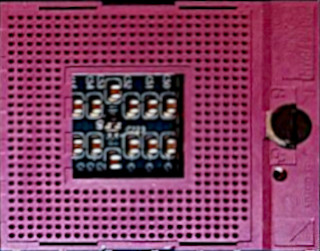
The Intel Core 2 Duo T7700 was a mobile processor with 2 cores, launched in May 2007. It is part of the Core 2 Duo lineup, using the Merom architecture with Socket P. Core 2 Duo T7700 has 4 MB of L2 cache and operates at 2.4 GHz. Intel is building the Core 2 Duo T7700 on a 65 nm production process using 293 million transistors. The multiplier is locked on Core 2 Duo T7700, which limits its overclocking capabilities.
With a TDP of 35 W, the Core 2 Duo T7700 consumes only little energy.
The SSE4 instruction set is not supported, which can cause problems with modern games, as they require that capability. Hardware virtualization is available on the Core 2 Duo T7700, which greatly improves virtual machine performance.
Physical
| Socket: | Intel Socket P |
|---|---|
| Foundry: | Intel |
| Process Size: | 65 nm |
| Transistors: | 293 million |
| Die Size: | 143 mm² |
| Package: | FC-PGA |
Processor
| Market: | Mobile |
|---|---|
| Production Status: | End-of-life |
| Release Date: | May 27th, 2007 |
| Part#: | SLA43 SLAF7 |
Performance
| Frequency: | 2.4 GHz |
|---|---|
| Turbo Clock: | N/A |
| Base Clock: | 200 MHz |
| Multiplier: | 12.0x |
| Multiplier Unlocked: | No |
| Voltage: | 1.3 V |
| TDP: | 35 W |
Architecture
| Codename: | Merom |
|---|---|
| Generation: |
Core 2 Duo
(Merom) |
| Memory Support: | unknown |
| ECC Memory: | No |
Core Config
| # of Cores: | 2 |
|---|---|
| # of Threads: | 2 |
| SMP # CPUs: | 1 |
| Integrated Graphics: | On certain motherboards (Chipset feature) |
Cache
| Cache L1: | 64 KB |
|---|---|
| Cache L2: | 4 MB |
Features
|
May 3rd, 2024 20:53 EDT
change timezone
Latest GPU Drivers
New Forum Posts
- Only some humans can see refresh rates faster than others, I am one of those humans. (4)
- NASA Achieves milestone Solid State Battery (213)
- TechPowerUp Screenshot Thread (MASSIVE 56K WARNING) (4215)
- Outer Worlds getting boring (37)
- Change GPU or PSU ? Games look cryspy and sharp with microsuttering (1)
- FINAL FANTASY XIV: Dawntrail Official Benchmark (80)
- Announcement: VPN's no longer work right in Windows 10 or 11 or Servers (33)
- Need advice for UPS that will be use only for bios updates (8)
- Ryzen 7800x3d $196 with bundle at Microcenter (27)
- 7800x3d $216 in bundle at Microcenter (39)
Popular Reviews
- ASRock NUC BOX-155H (Intel Core Ultra 7 155H) Review
- Meze Audio LIRIC 2nd Generation Closed-Back Headphones Review
- Finalmouse UltralightX Review
- Montech Sky Two GX Review
- Gigabyte GeForce RTX 4070 Ti Super Gaming OC Review
- Upcoming Hardware Launches 2023 (Updated Feb 2024)
- HYTE THICC Q60 240 mm AIO Review
- Alienware Pro Wireless Gaming Keyboard Review
- Ugreen NASync DXP4800 Plus Review
- Team Group T-Force Vulcan ECO DDR5-6000 32 GB CL38 Review
Controversial News Posts
- Intel Statement on Stability Issues: "Motherboard Makers to Blame" (235)
- Windows 11 Now Officially Adware as Microsoft Embeds Ads in the Start Menu (167)
- Sony PlayStation 5 Pro Specifications Confirmed, Console Arrives Before Holidays (117)
- AMD's RDNA 4 GPUs Could Stick with 18 Gbps GDDR6 Memory (114)
- AMD to Redesign Ray Tracing Hardware on RDNA 4 (113)
- NVIDIA Points Intel Raptor Lake CPU Users to Get Help from Intel Amid System Instability Issues (106)
- AMD "Strix Halo" Zen 5 Mobile Processor Pictured: Chiplet-based, Uses 256-bit LPDDR5X (103)
- AMD Ryzen 9 7900X3D Now at a Mouth-watering $329 (103)