Report an Error


AMD Capilano
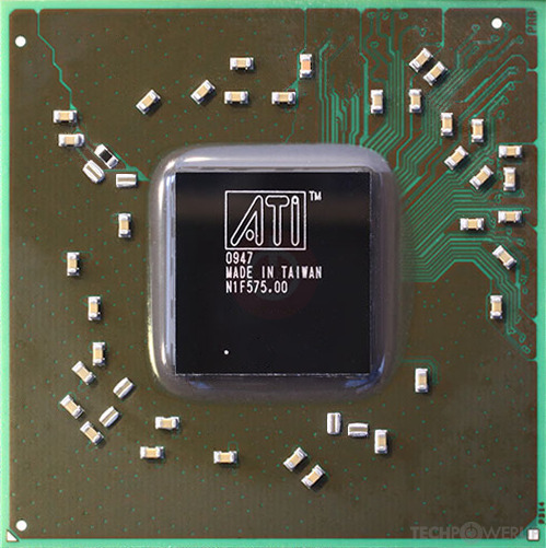
Capilano

Block Diagram
AMD's Capilano GPU uses the TeraScale 2 architecture and is made using a 40 nm production process at TSMC. With a die size of 104 mm² and a transistor count of 627 million it is a small chip. Capilano supports DirectX 11.2 (Feature Level 11_0). For GPU compute applications, OpenCL version 1.2 can be used. It features 400 shading units, 20 texture mapping units and 8 ROPs.
Further reading:
Evergreen Series Instruction Set Architecture 
Graphics Processor
- Released
- Oct 28th, 2009
- GPU Name
- Capilano
- Desktop Variant
- Redwood
- Generation
- Evergreen
- Architecture
- TeraScale 2
- Foundry
- TSMC
- Process Size
- 40 nm
- Transistors
- 627 million
- Density
- 6.0M / mm²
- Die Size
- 104 mm²
- Package
- FCBGA-962
Graphics Features
- DirectX
- 11.2 (11_0)
- OpenGL
- 4.4
- OpenCL
- 1.2
- Vulkan
- N/A
- Shader Model
- 5.0
- WDDM
- 1.3
- Compute
- GFX4
- DCE
- 4.0
- UVD
- 2.3
Render Config
- Shading Units
- 400
- TMUs
- 20
- ROPs
- 8
- Compute Units
- 5
- Z-Stencil
- 40
- L1 Cache
- 8 KB per CU
- L2 Cache
- 256 KB
- Max. TDP
- 30 W
All TeraScale 2 GPUs
- AMD Barts
- AMD Blackcomb
- ATI Broadway
- AMD Broadway
- AMD Caicos
- AMD Capilano
- ATI Cedar
- AMD Cedar
- ATI Cypress
- AMD Cypress
- AMD Granville
- ATI Hemlock
- AMD Juniper
- ATI Juniper
- AMD Latte
- AMD Lexington
- AMD Loveland
- ATI Madison
- AMD Onega
- ATI Park
- AMD Park
- ATI Pinewood
- AMD Pinewood
- ATI Redwood
- AMD Redwood
- AMD Robson
- AMD Seymour
- AMD Sumo
- AMD SuperSumo
- AMD Thames
- AMD Turks
- ATI Turks
- AMD Whistler
AMD GPU Architecture History
Graphics cards using the AMD Capilano GPU
| Name | Chip | Memory | Shaders | TMUs | ROPs | GPU Clock | Memory Clock |
|---|---|---|---|---|---|---|---|
| Capilano PRO | 1024 MB | 400 | 20 | 8 | 600 MHz | 900 MHz | |
| Capilano LP | 1024 MB | 400 | 20 | 8 | 450 MHz | 900 MHz | |
| Capilano XT | 1024 MB | 400 | 20 | 8 | 650 MHz | 800 MHz | |
| Capilano XT | 1024 MB | 400 | 20 | 8 | 600 MHz | 800 MHz |


Capilano GPU Notes
| Generation: Evergreen Desktop Variant: Redwood Graphics/Compute: GFX4 Display Core Engine: 4.0 Unified Video Decoder: 2.3 |
May 2nd, 2024 10:28 EDT
change timezone
Latest GPU Drivers
New Forum Posts
- Aviation fuel, no co2 (9)
- Old high quality PSU, or semi-old mid-quality PSU? (43)
- TPU's Nostalgic Hardware Club (18492)
- Ryzen Owners Zen Garden (7281)
- 7900 XTX Seriously lacking (104)
- need help with power limiting my i7-8750h (7)
- Share your AIDA 64 cache and memory benchmark here (2926)
- Would you guys be ok with 70C idle temp on NVME storage. (24)
- Are all software/scheduling issues with e-cores fixed on Intel 12th to 14th Gen - Willing to give hybrid ach a chance now (88)
- Current Sales, Bundles, Giveaways (10224)
Popular Reviews
- Ugreen NASync DXP4800 Plus Review
- ASRock NUC BOX-155H (Intel Core Ultra 7 155H) Review
- Montech Sky Two GX Review
- HYTE THICC Q60 240 mm AIO Review
- Upcoming Hardware Launches 2023 (Updated Feb 2024)
- MOONDROP x Crinacle DUSK In-Ear Monitors Review - The Last 5%
- Team Group T-Force Vulcan ECO DDR5-6000 32 GB CL38 Review
- AMD Ryzen 7 7800X3D Review - The Best Gaming CPU
- Thermalright Phantom Spirit 120 EVO Review
- ASUS Radeon RX 7900 GRE TUF OC Review
Controversial News Posts
- Intel Statement on Stability Issues: "Motherboard Makers to Blame" (225)
- Windows 11 Now Officially Adware as Microsoft Embeds Ads in the Start Menu (159)
- Sony PlayStation 5 Pro Specifications Confirmed, Console Arrives Before Holidays (117)
- AMD's RDNA 4 GPUs Could Stick with 18 Gbps GDDR6 Memory (109)
- NVIDIA Points Intel Raptor Lake CPU Users to Get Help from Intel Amid System Instability Issues (106)
- AMD "Strix Halo" Zen 5 Mobile Processor Pictured: Chiplet-based, Uses 256-bit LPDDR5X (103)
- AMD Ryzen 9 7900X3D Now at a Mouth-watering $329 (98)
- TechPowerUp Hiring: Reviewers Wanted for Motherboards, Laptops, Gaming Handhelds and Prebuilt Desktops (93)