Report an Error


ATI R360

R360
SIC66SIC66
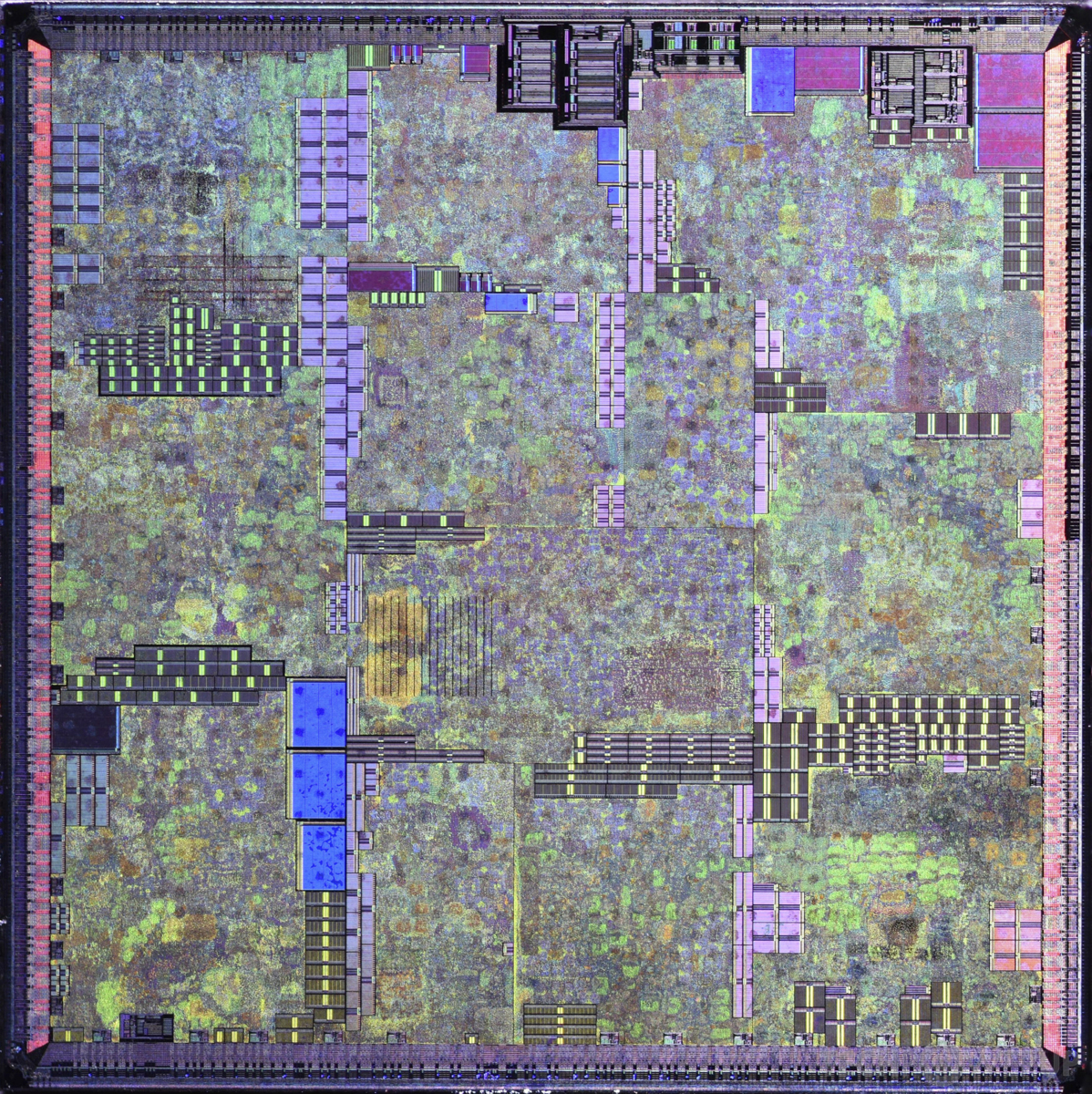
Die Shot
ATI's R360 GPU uses the R300 architecture and is made using a 150 nm production process at TSMC. With a die size of 218 mm² and a transistor count of 117 million it is a medium-sized chip. R360 supports DirectX 9.0. Modern GPU compute technologies are not available. It features 8 pixel shaders and 4 vertex shaders, 8 texture mapping units and 8 ROPs. Due to the lack of unified shaders you will not be able to run recent games at all (which require unified shader/DX10+ support).
Graphics Processor
- Released
- Mar 1st, 2003
- GPU Name
- R360
- Codename
- Khan
- Architecture
- R300
- Foundry
- TSMC
- Process Size
- 150 nm
- Transistors
- 117 million
- Density
- 536.7K / mm²
- Die Size
- 218 mm²
Graphics Features
- DirectX
- 9.0
- OpenGL
- 2.0
- OpenCL
- N/A
- Vulkan
- N/A
- Pixel Shader
- 2.0
- Vertex Shader
- 2.0
- WDDM
- 1.0
- Compute
- GFX2
Render Config
- Pixel Shaders
- 8
- Vertex Shaders
- 4
- TMUs
- 8
- ROPs
- 8
- Max. TDP
- 60 W
All R300 GPUs
ATI GPU Architecture History
Graphics cards using the ATI R360 GPU
| Name | Chip | Memory | Shaders | TMUs | ROPs | GPU Clock | Memory Clock |
|---|---|---|---|---|---|---|---|
| R360 | 256 MB | 8 / 4 | 8 | 8 | 412 MHz | 365 MHz | |
| R360 | 128 MB | 8 / 4 | 8 | 8 | 390 MHz | 338 MHz | |
| R360 GL | 256 MB | 8 / 4 | 8 | 8 | 412 MHz | 344 MHz | |
| R360 GL | 256 MB | 8 / 4 | 8 | 8 | 380 MHz | 350 MHz | |
| R360 | 256 MB | 8 / 4 | 8 | 8 | 380 MHz | 340 MHz | |
| R360 | 256 MB | 8 / 4 | 8 | 8 | 412 MHz | 365 MHz | |
| R360 | 128 MB | 8 / 4 | 8 | 8 | 378 MHz | 338 MHz |


R360 GPU Notes
| Codename: Khan Graphics/Compute: GFX2 Smart Shader 2.1 Smooth Vision 2.1 TruForm 2.0 FullStream Hyper Z III+ Video Shader Video Immersion II Programmable pixel&vertex pipelines |
May 7th, 2024 08:43 EDT
change timezone
Latest GPU Drivers
New Forum Posts
- 6800XT Red Devil with 18°C difference from Core to Hotspot (4)
- The Official Thermal Interface Material thread (1172)
- Dota 2 GPU performance test (5)
- not impressed - nvme vs ssd (24)
- Only some humans can see refresh rates faster than others, I am one of those humans. (205)
- My new folding rig. (5)
- What are you playing? (20595)
- What's your latest tech purchase? (20458)
- VR/MR/AR Concert experiences (0)
- Minions Wi-Fi 6 and 6E (18)
Popular Reviews
- Finalmouse UltralightX Review
- Corsair iCUE Link RX120 RGB 120 mm Fan Review
- Cougar Hotrod Royal Gaming Chair Review
- Meze Audio LIRIC 2nd Generation Closed-Back Headphones Review
- Upcoming Hardware Launches 2023 (Updated Feb 2024)
- ASRock NUC BOX-155H (Intel Core Ultra 7 155H) Review
- AMD Ryzen 7 7800X3D Review - The Best Gaming CPU
- ASUS Radeon RX 7900 GRE TUF OC Review
- Montech Sky Two GX Review
- HYTE THICC Q60 240 mm AIO Review
Controversial News Posts
- Intel Statement on Stability Issues: "Motherboard Makers to Blame" (250)
- AMD to Redesign Ray Tracing Hardware on RDNA 4 (191)
- Windows 11 Now Officially Adware as Microsoft Embeds Ads in the Start Menu (167)
- NVIDIA to Only Launch the Flagship GeForce RTX 5090 in 2024, Rest of the Series in 2025 (122)
- Sony PlayStation 5 Pro Specifications Confirmed, Console Arrives Before Holidays (119)
- AMD's RDNA 4 GPUs Could Stick with 18 Gbps GDDR6 Memory (114)
- NVIDIA Points Intel Raptor Lake CPU Users to Get Help from Intel Amid System Instability Issues (106)
- AMD Ryzen 9 7900X3D Now at a Mouth-watering $329 (104)