Report an Error


ATI Rage 128 PRO
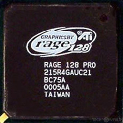
Rage 128 PRO

215R4GAUC21

Fritzchens Fritz
Die Shot
ATI's Rage 128 PRO GPU uses the Rage 4 architecture and is made using a 250 nm production process at UMC. With a die size of 98 mm² and a transistor count of 8 million it is a very small chip. Rage 128 PRO supports DirectX 6.0. Modern GPU compute technologies are not available. It features 2 pixel shaders and 0 vertex shaders, 2 texture mapping units and 2 ROPs. Due to the lack of unified shaders you will not be able to run recent games at all (which require unified shader/DX10+ support).
Graphics Processor
- Released
- Jun 16th, 1999
- GPU Name
- Rage 128 PRO
- Architecture
- Rage 4
- Foundry
- UMC
- Process Size
- 250 nm
- Transistors
- 8 million
- Density
- 81.6K / mm²
- Die Size
- 98 mm²
- Package
- BGA-328/329/385
Graphics Features
- DirectX
- 6.0
- OpenGL
- 1.2
- OpenCL
- N/A
- Vulkan
- N/A
- Pixel Shader
- N/A
- Vertex Shader
- N/A
Render Config
- Pixel Shaders
- 2
- Vertex Shaders
- 0
- TMUs
- 2
- ROPs
- 2
All Rage 4 GPUs
- ATI M1
- ATI M3
- ATI M4
- ATI Rage 128
- ATI Rage 128 PRO
- ATI Rage Mobility
ATI GPU Architecture History
Graphics cards using the ATI Rage 128 PRO GPU
| Name | Chip | Memory | Shaders | TMUs | ROPs | GPU Clock | Memory Clock |
|---|---|---|---|---|---|---|---|
| Rage 128 PRO | 32 MB | 2 / 0 | 2 | 2 | 125 MHz | 143 MHz | |
| Rage 128 PRO | 32 MB | 2 / 0 | 2 | 2 | 80 MHz | 120 MHz | |
| Rage 128 PRO | 32 MB | 2 / 0 | 2 | 2 | 118 MHz | 143 MHz | |
| Rage 128 PRO | 16 MB | 2 / 0 | 2 | 2 | 130 MHz | 130 MHz | |
| Rage 128 PRO | 32 MB | 2 / 0 | 2 | 2 | 120 MHz | 120 MHz | |
| Rage 128 PRO | 32 MB | 2 / 0 | 2 | 2 | 130 MHz | 130 MHz |


Rage 128 PRO GPU Notes
| Chip Codes: 215R4FAUC21 215R4GAUC21 215R4LAUC21 215R4UAUC21 |
May 5th, 2024 06:31 EDT
change timezone
Latest GPU Drivers
New Forum Posts
- Only some humans can see refresh rates faster than others, I am one of those humans. (117)
- Apparently Valve is giving refunds on Helldivers 2 regardless of hour count. Details inside. (38)
- Arctic MX-6 shelf life is just a couple months? (87)
- Is updating BIOS to beta versions a good idea if you have the most recent version installed but still face issues? (6)
- Resolution problems in-game with Av receiver (windows 11) (0)
- Unigine Heaven 4.0 Benchmark Scores Part 2 (931)
- AI Benchmark Alpha version 0.1.2 (2)
- Post your Speedometer 3.0 Score (38)
- What's your latest tech purchase? (20439)
- Strange system crashes out of nowhere, help (25)
Popular Reviews
- Finalmouse UltralightX Review
- Meze Audio LIRIC 2nd Generation Closed-Back Headphones Review
- ASRock NUC BOX-155H (Intel Core Ultra 7 155H) Review
- Montech Sky Two GX Review
- Cougar Hotrod Royal Gaming Chair Review
- Upcoming Hardware Launches 2023 (Updated Feb 2024)
- Alienware Pro Wireless Gaming Keyboard Review
- AMD Ryzen 7 7800X3D Review - The Best Gaming CPU
- HYTE THICC Q60 240 mm AIO Review
- Logitech G Pro X Superlight 2 Review - Updated with 4000 Hz Tested
Controversial News Posts
- Intel Statement on Stability Issues: "Motherboard Makers to Blame" (240)
- Windows 11 Now Officially Adware as Microsoft Embeds Ads in the Start Menu (167)
- AMD to Redesign Ray Tracing Hardware on RDNA 4 (138)
- Sony PlayStation 5 Pro Specifications Confirmed, Console Arrives Before Holidays (117)
- AMD's RDNA 4 GPUs Could Stick with 18 Gbps GDDR6 Memory (114)
- NVIDIA Points Intel Raptor Lake CPU Users to Get Help from Intel Amid System Instability Issues (106)
- AMD Ryzen 9 7900X3D Now at a Mouth-watering $329 (104)
- AMD "Strix Halo" Zen 5 Mobile Processor Pictured: Chiplet-based, Uses 256-bit LPDDR5X (103)