Report an Error


Dell GT 330
- Graphics Processor
- GT215
- Cores
- 96
- TMUs
- 32
- ROPs
- 8
- Memory Size
- 1024 MB
- Memory Type
- DDR3
- Bus Width
- 128 bit

GPU
Graphics Processor
Graphics Card
- Release Date
Feb 2nd, 2010
Feb 4th, 2010
- Generation
- GeForce 300
- Predecessor
- GeForce 200
- Successor
- GeForce 400
- Production
- End-of-life
- Bus Interface
- PCIe 2.0 x16
Clock Speeds
- GPU Clock
- 550 MHz
- Shader Clock
- 1340 MHz
- Memory Clock
-
1000 MHz
790 MHz (-21%)
2 Gbps effective
1580 Mbps effective
Memory
- Memory Size
-
512 MB
1024 MB
- Memory Type
GDDR3
DDR3
- Memory Bus
- 128 bit
- Bandwidth
-
32.00 GB/s
25.28 GB/s
Render Config
- Shading Units
- 96
- TMUs
- 32
- ROPs
- 8
- SM Count
- 12
- L2 Cache
- 64 KB
Theoretical Performance
- Pixel Rate
- 4.400 GPixel/s
- Texture Rate
- 17.60 GTexel/s
- FP32 (float)
- 257.3 GFLOPS
Board Design
- Slot Width
- Single-slot
- TDP
- 75 W
- Suggested PSU
- 250 W
- Outputs
1x DVI
1x HDMI
1x VGA
1x DVI
1x DisplayPort
- Power Connectors
- None
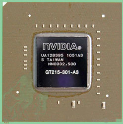
- Board Number
- P681 SKU 11
Graphics Features
- DirectX
- 11.1 (10_1)
- OpenGL
- 3.3
- OpenCL
- 1.1
- Vulkan
- N/A
- CUDA
- 1.2
- Shader Model
- 4.1
Card Notes
| Memory Variant: 1 GB |
GT215 GPU Notes
| PureVideo HD: VP4 VDPAU: Feature Set C |
Other retail boards based on this design (1)
| Name | GPU Clock | Memory Clock | Other Changes |
|---|---|---|---|
|
Dell GT 330

|
550 MHz | 790 MHz | 1024 MB, DDR3, 1x DVI 1x DisplayPort |
May 8th, 2024 12:46 EDT
change timezone
Latest GPU Drivers
New Forum Posts
- Does anyone here overclock their video cards? Is it really worth it? (61)
- Your way of cooling your PC? (28)
- PSU making a clicking sound, PC wont turn on (20)
- not impressed - nvme vs ssd (61)
- Free Games Thread (3791)
- Urgent: PC wont turn on with PSU connected to MOBO (24)
- High c0% and system idle process (3)
- 1GHZ less than I should be getting (9)
- POLL: Can you see the difference past 60fps (gaming/other) (49)
- Dell Workstation Owners Club (3064)
Popular Reviews
- CHERRY XTRFY M64 Pro Review
- Corsair iCUE Link RX120 RGB 120 mm Fan Review
- Finalmouse UltralightX Review
- Upcoming Hardware Launches 2023 (Updated Feb 2024)
- Cougar Hotrod Royal Gaming Chair Review
- Meze Audio LIRIC 2nd Generation Closed-Back Headphones Review
- AMD Ryzen 7 7800X3D Review - The Best Gaming CPU
- ASRock NUC BOX-155H (Intel Core Ultra 7 155H) Review
- ASUS Radeon RX 7900 GRE TUF OC Review
- Sapphire Radeon RX 7900 GRE Pulse Review
Controversial News Posts
- Intel Statement on Stability Issues: "Motherboard Makers to Blame" (261)
- AMD to Redesign Ray Tracing Hardware on RDNA 4 (205)
- Windows 11 Now Officially Adware as Microsoft Embeds Ads in the Start Menu (167)
- NVIDIA to Only Launch the Flagship GeForce RTX 5090 in 2024, Rest of the Series in 2025 (142)
- Sony PlayStation 5 Pro Specifications Confirmed, Console Arrives Before Holidays (119)
- AMD's RDNA 4 GPUs Could Stick with 18 Gbps GDDR6 Memory (114)
- NVIDIA Points Intel Raptor Lake CPU Users to Get Help from Intel Amid System Instability Issues (106)
- AMD Ryzen 9 7900X3D Now at a Mouth-watering $329 (104)