Report an Error


NVIDIA GeForce FX 5500
- Graphics Processor
- NV34B
- Pixel Shaders
- 4
- Vertex Shaders
- 2
- TMUs
- 4
- ROPs
- 4
- Memory Size
- 64 MB
- Memory Type
- DDR
- Bus Width
- 128 bit

GPU
Recommended Gaming Resolutions:
- 640x480
- 1280x720
- 1366x768
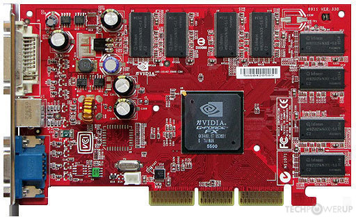
The GeForce FX 5500 was a graphics card by NVIDIA, launched on March 17th, 2004. Built on the 150 nm process, and based on the NV34B graphics processor, in its FX 5500 variant, the card supports DirectX 9.0a. Since GeForce FX 5500 does not support DirectX 11 or DirectX 12, it might not be able to run all the latest games. The NV34B graphics processor is a relatively small chip with a die area of only 91 mm² and 45 million transistors. It features 4 pixel shaders and 2 vertex shaders, 4 texture mapping units, and 4 ROPs. Due to the lack of unified shaders you will not be able to run recent games at all (which require unified shader/DX10+ support). NVIDIA has paired 64 MB DDR memory with the GeForce FX 5500, which are connected using a 128-bit memory interface. The GPU is operating at a frequency of 270 MHz, memory is running at 166 MHz.
Being a single-slot card, the NVIDIA GeForce FX 5500 does not require any additional power connector, its power draw is not exactly known. Display outputs include: 1x DVI, 1x VGA, 1x S-Video. GeForce FX 5500 is connected to the rest of the system using an AGP 8x interface. The card measures 152 mm in length, and features a single-slot cooling solution.
Being a single-slot card, the NVIDIA GeForce FX 5500 does not require any additional power connector, its power draw is not exactly known. Display outputs include: 1x DVI, 1x VGA, 1x S-Video. GeForce FX 5500 is connected to the rest of the system using an AGP 8x interface. The card measures 152 mm in length, and features a single-slot cooling solution.
Graphics Processor
Graphics Card
- Release Date
- Mar 17th, 2004
- Generation
-
GeForce FX
(5500)
- Predecessor
- GeForce 4 Ti
- Successor
- GeForce 6 AGP
- Production
- End-of-life
- Bus Interface
- AGP 8x
Clock Speeds
- GPU Clock
- 270 MHz
- Memory Clock
-
166 MHz
332 Mbps effective
Memory
- Memory Size
- 64 MB
- Memory Type
- DDR
- Memory Bus
- 128 bit
- Bandwidth
- 5.312 GB/s
Render Config
- Pixel Shaders
- 4
- Vertex Shaders
- 2
- TMUs
- 4
- ROPs
- 4
Theoretical Performance
- Pixel Rate
- 1.080 GPixel/s
- Vertex Rate
- 135.0 MVertices/s
- Texture Rate
- 1.080 GTexel/s
Board Design
- Slot Width
- Single-slot
- Length
- 152 mm
6 inches
- TDP
- unknown
- Suggested PSU
- 200 W
- Outputs
- 1x DVI
1x VGA
1x S-Video
- Power Connectors
- None
Graphics Features
- DirectX
- 9.0a
- OpenGL
-
1.5 (full)
2.0 (partial)
- OpenCL
- N/A
- Vulkan
- N/A
- Pixel Shader
- 2.0a
- Vertex Shader
- 2.0a
Card Notes
| Variant Memory: 128 MB Variant Memory: 256 MB |
NV34B GPU Notes
| OpenGL 2.0: 60% Support |
Retail boards based on this design (3)
| Name | GPU Clock | Memory Clock | Other Changes |
|---|---|---|---|
| 270 MHz | 200 MHz | 256 MB | |
| 240 MHz | 166 MHz | 256 MB | |
| 270 MHz | 200 MHz | 256 MB |


Apr 29th, 2024 19:12 EDT
change timezone
Latest GPU Drivers
New Forum Posts
- Have you got pie today? (16321)
- Milestones (13875)
- WCG Daily Numbers (12501)
- 7900 XTX Seriously lacking (16)
- TPU's Rosetta Milestones and Daily Pie Thread (1863)
- What's your latest tech purchase? (20396)
- Folding Pie and Milestones!! (9012)
- Is it better for zero RPM PSUs to place the fan on top? (30)
- Guide to proper case airflow design (30)
- i7-1355U (9)
Popular Reviews
- Ugreen NASync DXP4800 Plus Review
- HYTE THICC Q60 240 mm AIO Review
- Upcoming Hardware Launches 2023 (Updated Feb 2024)
- MOONDROP x Crinacle DUSK In-Ear Monitors Review - The Last 5%
- Team Group T-Force Vulcan ECO DDR5-6000 32 GB CL38 Review
- AMD Ryzen 7 7800X3D Review - The Best Gaming CPU
- Thermalright Phantom Spirit 120 EVO Review
- FiiO K19 Desktop DAC/Headphone Amplifier Review
- ASUS Radeon RX 7900 GRE TUF OC Review
- Sapphire Radeon RX 7900 GRE Pulse Review
Controversial News Posts
- Windows 11 Now Officially Adware as Microsoft Embeds Ads in the Start Menu (152)
- Intel Statement on Stability Issues: "Motherboard Makers to Blame" (152)
- Sony PlayStation 5 Pro Specifications Confirmed, Console Arrives Before Holidays (117)
- NVIDIA Points Intel Raptor Lake CPU Users to Get Help from Intel Amid System Instability Issues (106)
- AMD's RDNA 4 GPUs Could Stick with 18 Gbps GDDR6 Memory (105)
- AMD "Strix Halo" Zen 5 Mobile Processor Pictured: Chiplet-based, Uses 256-bit LPDDR5X (103)
- US Government Wants Nuclear Plants to Offload AI Data Center Expansion (98)
- TechPowerUp Hiring: Reviewers Wanted for Motherboards, Laptops, Gaming Handhelds and Prebuilt Desktops (90)