Report an Error

NVIDIA GeForce FX 5950 Ultra
- Graphics Processor
- NV38
- Pixel Shaders
- 4
- Vertex Shaders
- 3
- TMUs
- 8
- ROPs
- 4
- Memory Size
- 256 MB
- Memory Type
- DDR
- Bus Width
- 256 bit

GPU
Recommended Gaming Resolutions:
- 640x480
- 1280x720
- 1366x768
The GeForce FX 5950 Ultra was a high-end graphics card by NVIDIA, launched on October 23rd, 2003. Built on the 130 nm process, and based on the NV38 graphics processor, in its FX 5950 Ultra variant, the card supports DirectX 9.0a. Since GeForce FX 5950 Ultra does not support DirectX 11 or DirectX 12, it might not be able to run all the latest games. The NV38 graphics processor is an average sized chip with a die area of 207 mm² and 135 million transistors. It features 4 pixel shaders and 3 vertex shaders, 8 texture mapping units, and 4 ROPs. Due to the lack of unified shaders you will not be able to run recent games at all (which require unified shader/DX10+ support). NVIDIA has paired 256 MB DDR memory with the GeForce FX 5950 Ultra, which are connected using a 256-bit memory interface. The GPU is operating at a frequency of 475 MHz, memory is running at 475 MHz.
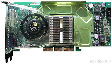
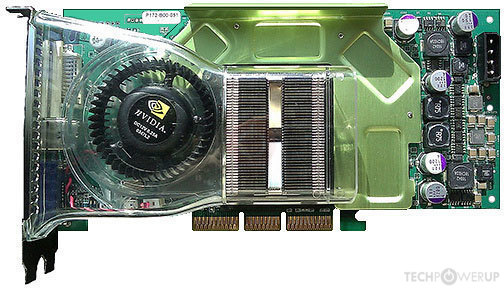
Being a dual-slot card, the NVIDIA GeForce FX 5950 Ultra draws power from 1x Molex power connector, with power draw rated at 74 W maximum. Display outputs include: 1x DVI, 1x VGA, 1x S-Video. GeForce FX 5950 Ultra is connected to the rest of the system using an AGP 8x interface. The card measures 229 mm in length, 111 mm in width, and features a dual-slot cooling solution. Its price at launch was 499 US Dollars.
Being a dual-slot card, the NVIDIA GeForce FX 5950 Ultra draws power from 1x Molex power connector, with power draw rated at 74 W maximum. Display outputs include: 1x DVI, 1x VGA, 1x S-Video. GeForce FX 5950 Ultra is connected to the rest of the system using an AGP 8x interface. The card measures 229 mm in length, 111 mm in width, and features a dual-slot cooling solution. Its price at launch was 499 US Dollars.
Graphics Processor
Graphics Card
- Release Date
- Oct 23rd, 2003
- Generation
-
GeForce FX
(5900)
- Predecessor
- GeForce 4 Ti
- Successor
- GeForce 6 AGP
- Production
- End-of-life
- Launch Price
- 499 USD
- Bus Interface
- AGP 8x
- Reviews
- 1 in our database
Clock Speeds
- GPU Clock
- 475 MHz
- Memory Clock
-
475 MHz
950 Mbps effective
Memory
- Memory Size
- 256 MB
- Memory Type
- DDR
- Memory Bus
- 256 bit
- Bandwidth
- 30.40 GB/s
Render Config
- Pixel Shaders
- 4
- Vertex Shaders
- 3
- TMUs
- 8
- ROPs
- 4
Theoretical Performance
- Pixel Rate
- 1.900 GPixel/s
- Vertex Rate
- 356.3 MVertices/s
- Texture Rate
- 3.800 GTexel/s
Board Design
- Slot Width
- Dual-slot
- Length
- 229 mm
9 inches
- Width
- 111 mm
4.4 inches
- TDP
- 74 W
- Suggested PSU
- 250 W
- Outputs
- 1x DVI
1x VGA
1x S-Video
- Power Connectors
- 1x Molex
Graphics Features
- DirectX
- 9.0a
- OpenGL
-
1.5 (full)
2.0 (partial)
- OpenCL
- N/A
- Vulkan
- N/A
- Pixel Shader
- 2.0a
- Vertex Shader
- 2.0a
Retail boards based on this design (2)
| Name | GPU Clock | Memory Clock | Other Changes |
|---|---|---|---|
| 475 MHz | 475 MHz | Single-slot | |
| 475 MHz | 475 MHz | Single-slot |


May 16th, 2024 01:19 EDT
change timezone
Latest GPU Drivers
New Forum Posts
- NVcleanstall error (1)
- Youtube, Discord, Visual Studio Code are flickering with black checkered squares/vertical lines. Partial solutions to this issue. (401)
- Post your Cinebench 2024 score (461)
- Air makes its way from the reservoir into the radiator. (81)
- FID when c-state is enabled (2)
- Is it normal to hear this sound coming from the psu? (35)
- Ryzen Owners Zen Garden (7365)
- The Official Thermal Interface Material thread (1191)
- Would you pay more for hardware with AI capabilities? (19)
- LOL ASUS says this is $200 in repair, Steve from gamers Nexus smokes ASUS, Steam Deck til I die boys!!!! (81)
Popular Reviews
- Homeworld 3 Performance Benchmark Review - 35 GPUs Tested
- Enermax REVOLUTION D.F. X 1200 W Review
- Upcoming Hardware Launches 2023 (Updated Feb 2024)
- Lofree Edge Ultra-Low Profile Wireless Mechanical Keyboard Review
- ZMF Caldera Closed Planar Magnetic Headphones Review
- AMD Ryzen 7 7800X3D Review - The Best Gaming CPU
- Corsair MP700 Pro SE 4 TB Review
- ASUS Radeon RX 7900 GRE TUF OC Review
- ThundeRobot ML903 NearLink Review
- Sapphire Radeon RX 7900 GRE Pulse Review
Controversial News Posts
- Intel Statement on Stability Issues: "Motherboard Makers to Blame" (267)
- AMD to Redesign Ray Tracing Hardware on RDNA 4 (227)
- Windows 11 Now Officially Adware as Microsoft Embeds Ads in the Start Menu (172)
- NVIDIA to Only Launch the Flagship GeForce RTX 5090 in 2024, Rest of the Series in 2025 (152)
- AMD Hits Highest-Ever x86 CPU Market Share in Q1 2024 Across Desktop and Server (137)
- AMD RDNA 5 a "Clean Sheet" Graphics Architecture, RDNA 4 Merely Corrects a Bug Over RDNA 3 (124)
- AMD's RDNA 4 GPUs Could Stick with 18 Gbps GDDR6 Memory (114)
- AMD Ryzen 9 7900X3D Now at a Mouth-watering $329 (104)