Report an Error
Intel Ironlake

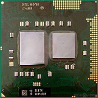
Ironlake
Intel's Ironlake GPU uses the Generation 5.75 architecture and is made using a 45 nm production process at Intel. With a die size of 114 mm² and a transistor count of 177 million it is a small chip. Ironlake supports DirectX 10.1. Modern GPU compute technologies are not available. It features 96 shading units, 16 texture mapping units and 2 ROPs.
Graphics Processor
- Released
- Jan 10th, 2010
- GPU Name
- Ironlake
- Architecture
- Generation 5.75
- Foundry
- Intel
- Process Size
- 45 nm
- Transistors
- 177 million
- Density
- 1.6M / mm²
- Die Size
- 114 mm²
Graphics Features
- DirectX
- 10.1
- OpenGL
- 2.1
- OpenCL
- N/A
- Vulkan
- N/A
- Shader Model
- 4.1
Render Config
- Shading Units
- 96
- TMUs
- 16
- ROPs
- 2
- Execution Units
- 16
- Max. TDP
- 35 W
All Generation 5.75 GPUs
- Intel Ironlake
Intel GPU Architecture History
- 2023 Xe-LPG
- 2022-2023 Generation 12.7
- 2021-2024 Generation 12.5
- 2021-2023 Generation 12.2
- 2020-2021 Generation 12.1
- 2019-2021 Generation 11.0
- 2016-2020 Generation 9.5
- 2015-2016 Generation 9.0
- 2014-2015 Generation 8.0
- 2013 Generation 7.5
- 2012-2013 Generation 7.0
- 2011 Generation 6.0
- 2010-2013 Knights
- 2010 Generation 5.75
- 2008-2010 PowerVR SGX545
- 2008 Generation 5.0
- 2008-2010 PowerVR SGX535
- 2006-2007 Generation 4.0
- 2005-2006 Generation 3.5
- 2004-2005 Generation 3.0
- 2002-2003 Generation 2.0
- 1998 i740
- 1998-2002 Generation 1.0
Graphics cards using the Intel Ironlake GPU
| Name | Chip | Memory | Shaders | TMUs | ROPs | Base Clock | Boost Clock | Memory Clock |
|---|---|---|---|---|---|---|---|---|
| System Shared | 96 | 16 | 2 | 133 MHz | 500 MHz | System Shared | ||
| System Shared | 96 | 12 | 2 | 533 MHz | System Shared |

Ironlake GPU Notes
| Arrandale Processors Clarkdale Processors |
May 23rd, 2024 00:23 EDT
change timezone
Latest GPU Drivers
New Forum Posts
- The Official Thermal Interface Material thread (1213)
- BSOD and Memory Errors (3)
- 95 cpu temp on idle and bios (3)
- x670e aorus pro x VGA led on but everything is working as intended. (2)
- CPU capped to 3/4 of full speed for no apparent reason on Lenovo Legion laptops (1)
- Removing the 12v sensing line on the thor 1200 (oringial) (1)
- Throttlestop - change profile does not change setting in TPL (14)
- Undervolt doesn't work? (7)
- Can anyone ID this fan? (prop only, no markings - super challenge!) (12)
- MSI laptop i9-13980HX limited to 3.7Ghz/115W! NO LIMITS, NO THROTTLING in TS (3)
Popular Reviews
- Ghost of Tsushima Performance Benchmark Review - 35 GPUs Tested
- Senua's Saga: Hellblade II Performance Benchmark Review
- Ghost of Tsushima: DLSS vs. FSR vs. XeSS Comparison Review
- PNY XLR8 Gaming EPIC-X RGB DDR5-6400 CL32 32 GB Review
- CHERRY XTRFY M68 Pro Review
- Upcoming Hardware Launches 2023 (Updated Feb 2024)
- TerraMaster D8 Hybrid Review
- Homeworld 3 Performance Benchmark Review - 35 GPUs Tested
- PMG Audio Apx In-Ear Monitors Review - $6500 Flagship!
- Silverstone Shark Force 120 mm Fan Review
Controversial News Posts
- Intel Statement on Stability Issues: "Motherboard Makers to Blame" (272)
- AMD to Redesign Ray Tracing Hardware on RDNA 4 (227)
- Windows 11 Now Officially Adware as Microsoft Embeds Ads in the Start Menu (173)
- NVIDIA to Only Launch the Flagship GeForce RTX 5090 in 2024, Rest of the Series in 2025 (154)
- AMD Hits Highest-Ever x86 CPU Market Share in Q1 2024 Across Desktop and Server (140)
- AMD RDNA 5 a "Clean Sheet" Graphics Architecture, RDNA 4 Merely Corrects a Bug Over RDNA 3 (139)
- AMD's RDNA 4 GPUs Could Stick with 18 Gbps GDDR6 Memory (114)
- AMD Ryzen 9 7900X3D Now at a Mouth-watering $329 (104)