Report an Error


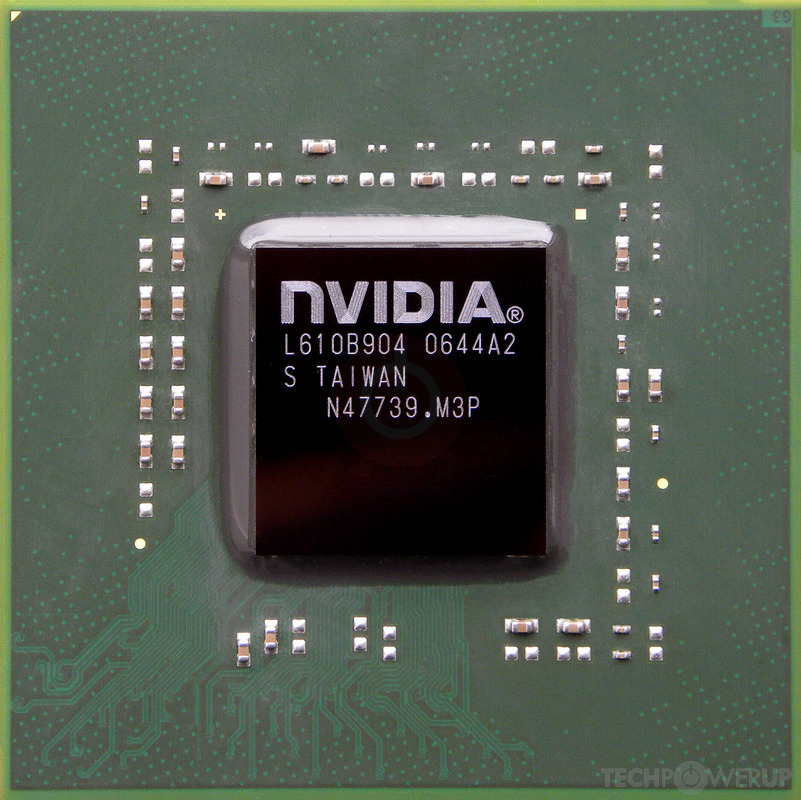
NVIDIA GeForce Go 7900 GS
- Graphics Processor
- G71
- Pixel Shaders
- 20
- Vertex Shaders
- 7
- TMUs
- 20
- ROPs
- 16
- Memory Size
- 512 MB
- Memory Type
- GDDR3
- Bus Width
- 256 bit

GPU
Graphics Processor
Mobile Graphics
- Release Date
- Apr 18th, 2006
- Generation
-
GeForce Go 7
(Go 7000)
- Predecessor
- GeForce Go 6
- Successor
- GeForce 8M
- Production
- End-of-life
- Bus Interface
- MXM-II
Clock Speeds
- GPU Clock
- 375 MHz
- Memory Clock
-
500 MHz
1000 Mbps effective
Memory
- Memory Size
-
256 MB
512 MB
- Memory Type
- GDDR3
- Memory Bus
- 256 bit
- Bandwidth
- 32.00 GB/s
Render Config
- Pixel Shaders
- 20
- Vertex Shaders
- 7
- TMUs
- 20
- ROPs
- 16
Theoretical Performance
- Pixel Rate
- 6.000 GPixel/s
- Vertex Rate
- 656.3 MVertices/s
- Texture Rate
- 7.500 GTexel/s
Board Design
- Slot Width
- MXM Module
- TDP
- 20 W
- Outputs
- Portable Device Dependent
Graphics Features
- DirectX
- 9.0c (9_3)
- OpenGL
-
2.1.2 (full)
3.x (partial)
- OpenCL
- N/A
- Vulkan
- N/A
- Shader Model
- 3.0
G71 GPU Notes
| PureVideo HD: VP1 VDPAU: No Support |
Other retail boards based on this design (1)
| Name | GPU Clock | Memory Clock | Other Changes |
|---|---|---|---|
|
NVIDIA GeForce Go 7900 GS

|
375 MHz | 500 MHz | 512 MB |
May 20th, 2024 18:39 EDT
change timezone
Latest GPU Drivers
New Forum Posts
- My anti budget PC (44)
- Inland 512GB SATA SSD; reliable? (6)
- For general use - moving files around and playing games, would you have an Optane boot drive or PCie gen 5? (55)
- GTA VI Now Slated For Launch in Fall of Next Year (1)
- TPU's Nostalgic Hardware Club (18514)
- What's your latest tech purchase? (20595)
- Fractal define R4 vs R5 build quality. (18)
- Samsung 870 EVO - Beware, certain batches prone to failure! (1134)
- Battery swap for cyberpower UPS (91)
- What are you playing? (20716)
Popular Reviews
- Ghost of Tsushima Performance Benchmark Review - 35 GPUs Tested
- TerraMaster D8 Hybrid Review
- Silverstone Shark Force 120 mm Fan Review
- Ghost of Tsushima: DLSS vs. FSR vs. XeSS Comparison Review
- Lofree Edge Ultra-Low Profile Wireless Mechanical Keyboard Review
- Homeworld 3 Performance Benchmark Review - 35 GPUs Tested
- PNY XLR8 Gaming EPIC-X RGB DDR5-6400 CL32 32 GB Review
- Upcoming Hardware Launches 2023 (Updated Feb 2024)
- Sapphire Radeon RX 7700 XT Pure Review
- AMD Ryzen 7 7800X3D Review - The Best Gaming CPU
Controversial News Posts
- Intel Statement on Stability Issues: "Motherboard Makers to Blame" (269)
- AMD to Redesign Ray Tracing Hardware on RDNA 4 (227)
- Windows 11 Now Officially Adware as Microsoft Embeds Ads in the Start Menu (173)
- NVIDIA to Only Launch the Flagship GeForce RTX 5090 in 2024, Rest of the Series in 2025 (154)
- AMD Hits Highest-Ever x86 CPU Market Share in Q1 2024 Across Desktop and Server (140)
- AMD RDNA 5 a "Clean Sheet" Graphics Architecture, RDNA 4 Merely Corrects a Bug Over RDNA 3 (139)
- AMD's RDNA 4 GPUs Could Stick with 18 Gbps GDDR6 Memory (114)
- AMD Ryzen 9 7900X3D Now at a Mouth-watering $329 (104)