Report an Error


NVIDIA NV25
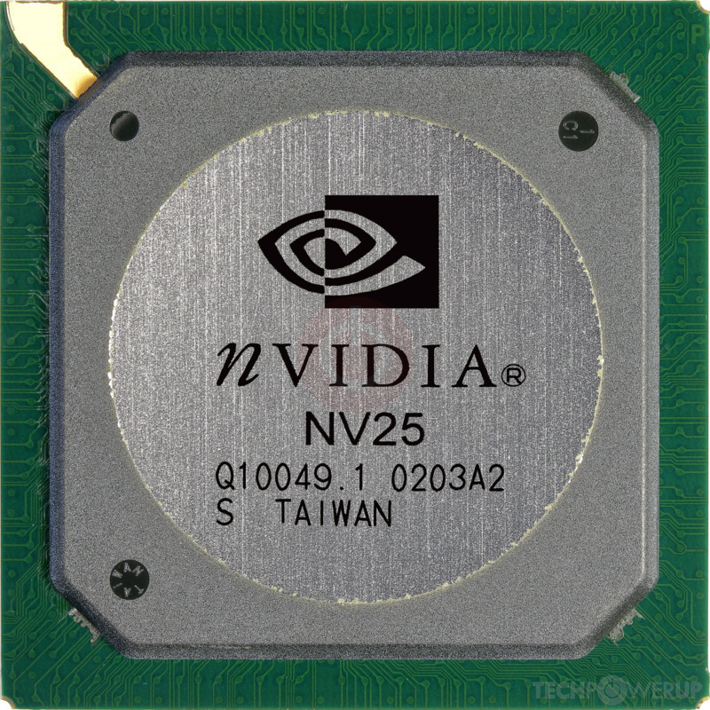
NV25

Ti 4200

Ti 4600

Die Shot
NVIDIA's NV25 GPU uses the Kelvin architecture and is made using a 150 nm production process at TSMC. With a die size of 142 mm² and a transistor count of 63 million it is a small chip. NV25 supports DirectX 8.1. For GPU compute applications, OpenCL version N/A can be used. It features 4 pixel shaders and 2 vertex shaders, 8 texture mapping units and 8 ROPs. Due to the lack of unified shaders you will not be able to run recent games at all (which require unified shader/DX10+ support).
Graphics Processor
- Released
- Feb 6th, 2002
- GPU Name
- NV25
- Architecture
- Kelvin
- Foundry
- TSMC
- Process Size
- 150 nm
- Transistors
- 63 million
- Density
- 443.7K / mm²
- Die Size
- 142 mm²
Graphics Features
- DirectX
- 8.1
- OpenGL
- 1.5
- OpenCL
- N/A
- Vulkan
- N/A
- Pixel Shader
- 1.3
- Vertex Shader
- 1.1
Render Config
- Pixel Shaders
- 4
- Vertex Shaders
- 2
- TMUs
- 8
- ROPs
- 8
All Kelvin GPUs
- NVIDIA NV20
- NVIDIA NV25
- NVIDIA NV28
- NVIDIA NV2A
- NVIDIA NV2A-B
NVIDIA GPU Architecture History
- 2024 Blackwell
- 2023 Hopper
- 2022-2024 Ada Lovelace
- 2020-2024 Ampere
- 2018-2022 Turing
- 2017-2020 Volta
- 2016-2021 Pascal
- 2014-2019 Maxwell 2.0
- 2014-2017 Maxwell
- 2013-2015 Kepler 2.0
- 2012-2018 Kepler
- 2010-2016 Fermi 2.0
- 2010-2013 VLIW Vec4
- 2010-2016 Fermi
- 2007-2013 Tesla 2.0
- 2006-2010 Tesla
- 2003-2013 Curie
- 2003-2005 Rankine
- 2001-2003 Kelvin
- 1999-2005 Celsius
- 1998-2000 Fahrenheit
Graphics cards using the NVIDIA NV25 GPU
| Name | Chip | Memory | Shaders | TMUs | ROPs | GPU Clock | Memory Clock |
|---|---|---|---|---|---|---|---|
| Ti 4600 | 128 MB | 4 / 2 | 8 | 4 | 300 MHz | 324 MHz | |
| 128 MB | 4 / 2 | 8 | 4 | 275 MHz | 275 MHz | ||
| NV25 GL | 128 MB | 4 / 2 | 8 | 8 | 300 MHz | 325 MHz | |
| NV25 GL | 64 MB | 4 / 2 | 8 | 8 | 275 MHz | 225 MHz | |
| NV25 GL | 128 MB | 4 / 2 | 8 | 8 | 275 MHz | 225 MHz | |
| Ti 4200 | 64 MB | 4 / 2 | 8 | 4 | 250 MHz | 250 MHz | |
| 64 MB | 4 / 2 | 8 | 4 | 250 MHz | 250 MHz |


May 7th, 2024 20:12 EDT
change timezone
Latest GPU Drivers
New Forum Posts
- POLL: Can you see the difference past 60fps (gaming/other) (1)
- Urgent: PC wont turn on with PSU connected to MOBO (10)
- I think my PC is underperforming (2)
- Apparently Valve is giving refunds on Helldivers 2 regardless of hour count. Details inside. (107)
- The Official Thermal Interface Material thread (1175)
- 1GHZ less than I should be getting (6)
- Only some humans can see refresh rates faster than others, I am one of those humans. (215)
- Share your AIDA 64 cache and memory benchmark here (2930)
- not impressed - nvme vs ssd (37)
- What are you playing? (20599)
Popular Reviews
- Corsair iCUE Link RX120 RGB 120 mm Fan Review
- CHERRY XTRFY M64 Pro Review
- Finalmouse UltralightX Review
- Cougar Hotrod Royal Gaming Chair Review
- Upcoming Hardware Launches 2023 (Updated Feb 2024)
- Meze Audio LIRIC 2nd Generation Closed-Back Headphones Review
- AMD Ryzen 7 7800X3D Review - The Best Gaming CPU
- ASRock NUC BOX-155H (Intel Core Ultra 7 155H) Review
- ASUS Radeon RX 7900 GRE TUF OC Review
- Sapphire Radeon RX 7900 GRE Pulse Review
Controversial News Posts
- Intel Statement on Stability Issues: "Motherboard Makers to Blame" (256)
- AMD to Redesign Ray Tracing Hardware on RDNA 4 (201)
- Windows 11 Now Officially Adware as Microsoft Embeds Ads in the Start Menu (167)
- NVIDIA to Only Launch the Flagship GeForce RTX 5090 in 2024, Rest of the Series in 2025 (131)
- Sony PlayStation 5 Pro Specifications Confirmed, Console Arrives Before Holidays (119)
- AMD's RDNA 4 GPUs Could Stick with 18 Gbps GDDR6 Memory (114)
- NVIDIA Points Intel Raptor Lake CPU Users to Get Help from Intel Amid System Instability Issues (106)
- AMD Ryzen 9 7900X3D Now at a Mouth-watering $329 (104)