Report an Error


NVIDIA Playstation 3 GPU 28nm
- Graphics Processor
- RSX-28nm
- Pixel Shaders
- 24
- Vertex Shaders
- 8
- TMUs
- 24
- ROPs
- 8
- Memory Size
- 256 MB
- Memory Type
- GDDR3
- Bus Width
- 128 bit
GPU

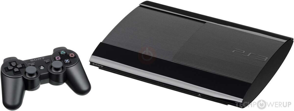
Front 2

Back
Recommended Gaming Resolutions:
- 640x480
- 1280x720
- 1366x768
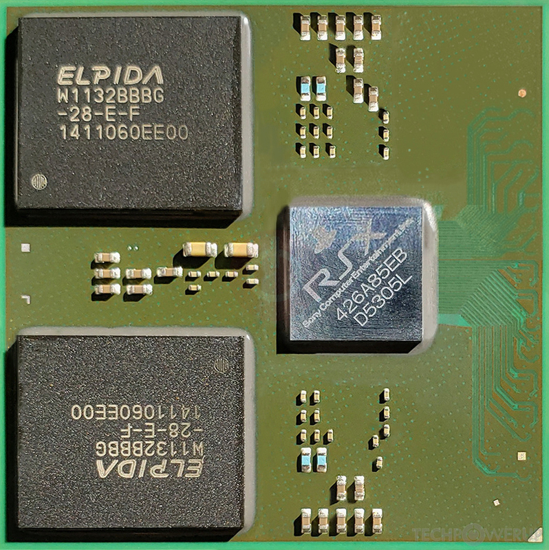
The Playstation 3 GPU 28nm was a performance-segment gaming console graphics solution by NVIDIA, launched on June 3rd, 2013. Built on the 28 nm process, and based on the RSX-28nm graphics processor, in its RSX-D5305L variant, the device does not support DirectX. The RSX-28nm graphics processor is a relatively small chip with a die area of only 68 mm² and 302 million transistors. It features 24 pixel shaders and 8 vertex shaders, 24 texture mapping units, and 8 ROPs. NVIDIA includes 256 MB GDDR3 memory, which are connected using a 128-bit memory interface. The GPU is operating at a frequency of 550 MHz, memory is running at 650 MHz.
Its power draw is rated at 21 W maximum. The console's dimensions are 290 mm x 60 mm x 230 mm, and it features a igp cooling solution. Its price at launch was 299 US Dollars.
Its power draw is rated at 21 W maximum. The console's dimensions are 290 mm x 60 mm x 230 mm, and it features a igp cooling solution. Its price at launch was 299 US Dollars.
Graphics Processor
Graphics Card
- Release Date
- Jun 3rd, 2013
- Generation
-
Console GPU
(Sony)
- Production
- End-of-life
- Launch Price
- 299 USD
Clock Speeds
- GPU Clock
- 550 MHz
- Memory Clock
-
650 MHz
1300 Mbps effective
Memory
- Memory Size
- 256 MB
- Memory Type
- GDDR3
- Memory Bus
- 128 bit
- Bandwidth
- 20.80 GB/s
Render Config
- Pixel Shaders
- 24
- Vertex Shaders
- 8
- TMUs
- 24
- ROPs
- 8
Theoretical Performance
- Pixel Rate
- 4.400 GPixel/s
- Vertex Rate
- 1.100 GVertices/s
- Texture Rate
- 13.20 GTexel/s
Board Design
- Length
- 290 mm
11.4 inches
- Width
- 60 mm
2.4 inches
- Height
- 230 mm
9.1 inches
- Weight
- 2.1 kg (4.6 lbs)
- TDP
- 21 W
- Outputs
- 1x HDMI 1.3
Graphics Features
- DirectX
- N/A
- OpenGL
- ES 1.1
- OpenCL
- N/A
- Vulkan
- N/A
- Pixel Shader
- 3.0
- Vertex Shader
- 3.0
Console Notes
| Playstation 3 Super Slim (5th Generation) 12GB CECH-43xxA = August 18th, 2013 250GB CECH-43xxB = August 18th, 2013 500GB CECH-43xxC = August 18th, 2013 |
RSX-28nm GPU Notes
| Multi-way programmable parallel floating-point shader pipelines Independent pixel/vertex shader architecture 24 parallel pixel-shader ALU pipes clocked @ 550 MHz 5 ALU operations per pipeline, per cycle - 2 vector4 - 2 scalar/dual/co-issue and fog ALU - 1 Texture ALU 16 floating-point operations per pipeline, per cycle Pixel Floating Point Operations: 211.2 GFLOPS (550MHz x 24 Shaders x 16 ops per clock per cycle) 8 parallel vertex pipelines @ 500 MHz 2 ALU operations per pipeline, per cycle - 1 vector4 - 1 scalar, dual issue 10 floating-point operations per pipeline, per cycle Vertex Floating Point Operations: 40.0 GFLOPS (500MHz x 8 Shaders x 10 ops per clock per cycle) Total Floating Point Operations: 251.2 GFLOPS (550MHz x 24 Shaders x 16 ops per clock per cycle) +(500MHz x 8 Shaders x 10 ops per clock per cycle) 74.0 billion shader operations/s (24 Pixel Shader Pipelines x 5 ALUs x 550 MHz) +(8 Vertex Shader Pipelines x 2 ALUs x 500 MHz) 24 texture filtering units (TF) 8 vertex texture addressing units (TA) 24 filtered samples per clock Peak texel fillrate: 13.2 GTexel/s (24 textures x 550 MHz) 32 unfiltered texture samples per clock (8 TA x 4 texture samples) 8 Render Output units / pixel rendering pipelines Peak pixel fillrate: 4.4 GPixel/s (8 ROPs x 550 MHz) Peak Z sample rate: 8.8 GSamples/s (2 Z-samples x 8 ROPs x 550 MHz) Peak Dot product operations: 56 billion/s (combined with Cell CPU) 128-bit pixel precision offers rendering of scenes with High dynamic range rendering (HDR) Cell FlexIO bus interface 20 GB/s read to the Cell and XDR memory 15 GB/s write to the Cell and XDR memory Support for PSGL (OpenGL ES 1.1 + Nvidia Cg) Support for S3TC texture compression |
May 16th, 2024 07:04 EDT
change timezone
Latest GPU Drivers
New Forum Posts
- EULA in Games (16)
- AIO Water Cooler vs Tower Air Cooler (18)
- Would you pay more for hardware with AI capabilities? (20)
- Ads in forums. under news (10)
- Ubuntu 24.04 LTS released (31)
- Homeworld 3 [Official Thread] (42)
- What's your latest tech purchase? (20533)
- Unknown Subvendor in GPU-Z (2)
- not impressed - nvme vs ssd (134)
- Last game you purchased? (297)
Popular Reviews
- Homeworld 3 Performance Benchmark Review - 35 GPUs Tested
- Enermax REVOLUTION D.F. X 1200 W Review
- Lofree Edge Ultra-Low Profile Wireless Mechanical Keyboard Review
- Upcoming Hardware Launches 2023 (Updated Feb 2024)
- ZMF Caldera Closed Planar Magnetic Headphones Review
- AMD Ryzen 7 7800X3D Review - The Best Gaming CPU
- Corsair MP700 Pro SE 4 TB Review
- ASUS Radeon RX 7900 GRE TUF OC Review
- ThundeRobot ML903 NearLink Review
- Sapphire Radeon RX 7900 GRE Pulse Review
Controversial News Posts
- Intel Statement on Stability Issues: "Motherboard Makers to Blame" (267)
- AMD to Redesign Ray Tracing Hardware on RDNA 4 (227)
- Windows 11 Now Officially Adware as Microsoft Embeds Ads in the Start Menu (172)
- NVIDIA to Only Launch the Flagship GeForce RTX 5090 in 2024, Rest of the Series in 2025 (152)
- AMD Hits Highest-Ever x86 CPU Market Share in Q1 2024 Across Desktop and Server (137)
- AMD RDNA 5 a "Clean Sheet" Graphics Architecture, RDNA 4 Merely Corrects a Bug Over RDNA 3 (126)
- AMD's RDNA 4 GPUs Could Stick with 18 Gbps GDDR6 Memory (114)
- AMD Ryzen 9 7900X3D Now at a Mouth-watering $329 (104)