Report an Error

ATI Radeon X700 PRO
- Graphics Processor
- RV410
- Pixel Shaders
- 8
- Vertex Shaders
- 6
- TMUs
- 8
- ROPs
- 8
- Memory Size
- 128 MB
- Memory Type
- GDDR3
- Bus Width
- 128 bit

GPU
Recommended Gaming Resolutions:
- 640x480
- 1280x720
- 1366x768
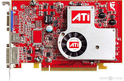
The Radeon X700 PRO was a mid-range graphics card by ATI, launched on September 1st, 2004. Built on the 110 nm process, and based on the RV410 graphics processor, in its RV410 PRO variant, the card supports DirectX 9.0b. Since Radeon X700 PRO does not support DirectX 11 or DirectX 12, it might not be able to run all the latest games. The RV410 graphics processor is an average sized chip with a die area of 156 mm² and 120 million transistors. It features 8 pixel shaders and 6 vertex shaders, 8 texture mapping units, and 8 ROPs. Due to the lack of unified shaders you will not be able to run recent games at all (which require unified shader/DX10+ support). ATI has paired 128 MB GDDR3 memory with the Radeon X700 PRO, which are connected using a 128-bit memory interface. The GPU is operating at a frequency of 425 MHz, memory is running at 430 MHz.
Being a single-slot card, the ATI Radeon X700 PRO does not require any additional power connector, its power draw is rated at 33 W maximum. Display outputs include: 1x DVI, 1x VGA, 1x S-Video. Radeon X700 PRO is connected to the rest of the system using a PCI-Express 1.0 x16 interface. The card's dimensions are 190 mm x 109 mm x 16 mm, and it features a single-slot cooling solution. Its price at launch was 179 US Dollars.
Being a single-slot card, the ATI Radeon X700 PRO does not require any additional power connector, its power draw is rated at 33 W maximum. Display outputs include: 1x DVI, 1x VGA, 1x S-Video. Radeon X700 PRO is connected to the rest of the system using a PCI-Express 1.0 x16 interface. The card's dimensions are 190 mm x 109 mm x 16 mm, and it features a single-slot cooling solution. Its price at launch was 179 US Dollars.
Graphics Processor
Graphics Card
- Release Date
- Sep 1st, 2004
- Generation
-
Radeon R400 PCIe
(X700)
- Predecessor
- Radeon R300
- Successor
- Radeon R500 PCIe
- Production
- End-of-life
- Launch Price
- 179 USD
- Bus Interface
- PCIe 1.0 x16
- Reviews
- 58 in our database
Clock Speeds
- GPU Clock
- 425 MHz
- Memory Clock
-
430 MHz
860 Mbps effective
Memory
- Memory Size
- 128 MB
- Memory Type
- GDDR3
- Memory Bus
- 128 bit
- Bandwidth
- 13.76 GB/s
Render Config
- Pixel Shaders
- 8
- Vertex Shaders
- 6
- TMUs
- 8
- ROPs
- 8
Theoretical Performance
- Pixel Rate
- 3.400 GPixel/s
- Vertex Rate
- 637.5 MVertices/s
- Texture Rate
- 3.400 GTexel/s
Board Design
- Slot Width
- Single-slot
- Length
- 190 mm
7.5 inches
- Width
- 109 mm
4.3 inches
- Height
- 16 mm
0.6 inches
- TDP
- 33 W
- Suggested PSU
- 200 W
- Outputs
- 1x DVI
1x VGA
1x S-Video
- Power Connectors
- None
- Board Number
- A379
Graphics Features
- DirectX
- 9.0b (9_2)
- OpenGL
- 2.0
- OpenCL
- N/A
- Vulkan
- N/A
- Pixel Shader
- 2.0b
- Vertex Shader
- 2.0b
Card Notes
| Variant Memory: 256 MB |
RV410 GPU Notes
| Mobile Variant: M26 Codename: Alto Graphics/Compute: GFX2 Smart Shader HD Smooth Vision HD TruForm 2.0 Hyper Z HD Video Shader HD 3Dc Compression Programmable pixel&vertex pipelines |
Retail boards based on this design (1)
| Name | GPU Clock | Memory Clock | Other Changes |
|---|---|---|---|
| 460 MHz | 480 MHz | 256 MB, Dual-slot |

May 2nd, 2024 23:05 EDT
change timezone
Latest GPU Drivers
New Forum Posts
- Need help with a persistent infection possible rootkit or other device. (12)
- Ryzen Owners Zen Garden (7286)
- The Official Thermal Interface Material thread (1137)
- Looking for recommendations to upgrade the GPU (38)
- ARDIYES RX 580 8gb Graphics Card (19)
- need help with power limiting my i7-8750h (9)
- 7800x3d $216 in bundle at Microcenter (31)
- FINAL FANTASY XIV: Dawntrail Official Benchmark (77)
- What's your latest tech purchase? (20415)
- Have you got pie today? (16324)
Popular Reviews
- HYTE THICC Q60 240 mm AIO Review
- ASRock NUC BOX-155H (Intel Core Ultra 7 155H) Review
- Montech Sky Two GX Review
- Ugreen NASync DXP4800 Plus Review
- Upcoming Hardware Launches 2023 (Updated Feb 2024)
- Meze Audio LIRIC 2nd Generation Closed-Back Headphones Review
- Team Group T-Force Vulcan ECO DDR5-6000 32 GB CL38 Review
- MOONDROP x Crinacle DUSK In-Ear Monitors Review - The Last 5%
- AMD Ryzen 7 7800X3D Review - The Best Gaming CPU
- Logitech G Pro X Superlight 2 Review - Updated with 4000 Hz Tested
Controversial News Posts
- Intel Statement on Stability Issues: "Motherboard Makers to Blame" (229)
- Windows 11 Now Officially Adware as Microsoft Embeds Ads in the Start Menu (166)
- Sony PlayStation 5 Pro Specifications Confirmed, Console Arrives Before Holidays (117)
- AMD's RDNA 4 GPUs Could Stick with 18 Gbps GDDR6 Memory (114)
- NVIDIA Points Intel Raptor Lake CPU Users to Get Help from Intel Amid System Instability Issues (106)
- AMD "Strix Halo" Zen 5 Mobile Processor Pictured: Chiplet-based, Uses 256-bit LPDDR5X (103)
- AMD Ryzen 9 7900X3D Now at a Mouth-watering $329 (103)
- TechPowerUp Hiring: Reviewers Wanted for Motherboards, Laptops, Gaming Handhelds and Prebuilt Desktops (93)