Report an Error


Sapphire HD 2600 XT Ultimate
- 11110-08-50
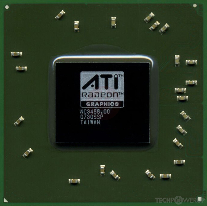
- Graphics Processor
- RV630
- Cores
- 120
- TMUs
- 8
- ROPs
- 4
- Memory Size
- 256 MB
- Memory Type
- GDDR3
- Bus Width
- 128 bit

GPU
Graphics Processor
Graphics Card
- Release Date
Jun 28th, 2007
Aug 6th, 2007
- Generation
-
Radeon R600
(HD 2600)
- Predecessor
- Radeon R500 PCIe
- Successor
- Radeon R700
- Production
- End-of-life
- Bus Interface
- PCIe 1.0 x16
Clock Speeds
- GPU Clock
- 800 MHz
- Memory Clock
-
700 MHz
1400 Mbps effective
Memory
- Memory Size
- 256 MB
- Memory Type
- GDDR3
- Memory Bus
- 128 bit
- Bandwidth
- 22.40 GB/s
Render Config
- Shading Units
- 120
- TMUs
- 8
- ROPs
- 4
- Compute Units
- 3
- L2 Cache
- 64 KB
Theoretical Performance
- Pixel Rate
- 3.200 GPixel/s
- Texture Rate
- 6.400 GTexel/s
- FP32 (float)
- 192.0 GFLOPS
Board Design
- Slot Width
- Single-slot
- TDP
- 45 W
- Suggested PSU
- 200 W
- Outputs
- 2x DVI
1x S-Video
- Power Connectors
- None
Graphics Features
- DirectX
- 10.0 (10_0)
- OpenGL
- 3.3
- OpenCL
- N/A
- Vulkan
- N/A
- Shader Model
- 4.0
Card Notes
| Variant Memory: 512 MB |
RV630 GPU Notes
| Mobile Variant: M76 Codename: Shaka Graphics/Compute: GFX3 Display Core Engine: 2.0 Unified Video Decoder: 1.0 RV630 Chip Numbers: RV630 XT (215CDABKA13FG) |
Other retail boards based on this design (2)
| Name | GPU Clock | Memory Clock | Other Changes |
|---|---|---|---|
| 830 MHz | 960 MHz | Dual-slot | |
|
Sapphire HD 2600 XT Ultimate

|
800 MHz | 700 MHz |

Apr 30th, 2024 18:27 EDT
change timezone
Latest GPU Drivers
New Forum Posts
- 7900 XTX Seriously lacking (77)
- TPU Merch (3)
- RX 7700 XT undervolting, power management and Adrenalin settings (1)
- Would you guys be ok with 70C idle temp on NVME storage. (17)
- Need help with a persistent infection possible rootkit or other device. (0)
- Is there a formula to help normalize temperature testing when ambient is variable? (16)
- RTX 4090? (30)
- Just for lolz, Post your 3DMark2001SE Benchmark scores! (81)
- problem with my 7900xtx (15)
- What's your latest tech purchase? (20400)
Popular Reviews
- Ugreen NASync DXP4800 Plus Review
- HYTE THICC Q60 240 mm AIO Review
- Team Group T-Force Vulcan ECO DDR5-6000 32 GB CL38 Review
- MOONDROP x Crinacle DUSK In-Ear Monitors Review - The Last 5%
- Upcoming Hardware Launches 2023 (Updated Feb 2024)
- Thermalright Phantom Spirit 120 EVO Review
- AMD Ryzen 7 7800X3D Review - The Best Gaming CPU
- FiiO K19 Desktop DAC/Headphone Amplifier Review
- ASUS Radeon RX 7900 GRE TUF OC Review
- AMD Ryzen 9 7950X3D Review - Best of Both Worlds
Controversial News Posts
- Intel Statement on Stability Issues: "Motherboard Makers to Blame" (191)
- Windows 11 Now Officially Adware as Microsoft Embeds Ads in the Start Menu (156)
- Sony PlayStation 5 Pro Specifications Confirmed, Console Arrives Before Holidays (117)
- AMD's RDNA 4 GPUs Could Stick with 18 Gbps GDDR6 Memory (109)
- NVIDIA Points Intel Raptor Lake CPU Users to Get Help from Intel Amid System Instability Issues (106)
- AMD "Strix Halo" Zen 5 Mobile Processor Pictured: Chiplet-based, Uses 256-bit LPDDR5X (103)
- US Government Wants Nuclear Plants to Offload AI Data Center Expansion (98)
- TechPowerUp Hiring: Reviewers Wanted for Motherboards, Laptops, Gaming Handhelds and Prebuilt Desktops (90)