Report an Error


NVIDIA Tesla S1075
- Graphics Processor
- GT200B x4
- Cores
- 240 x4
- TMUs
- 80 x4
- ROPs
- 32 x4
- Memory Size
- 4 GB x4
- Memory Type
- GDDR3
- Bus Width
- 512 bit x4

GPU
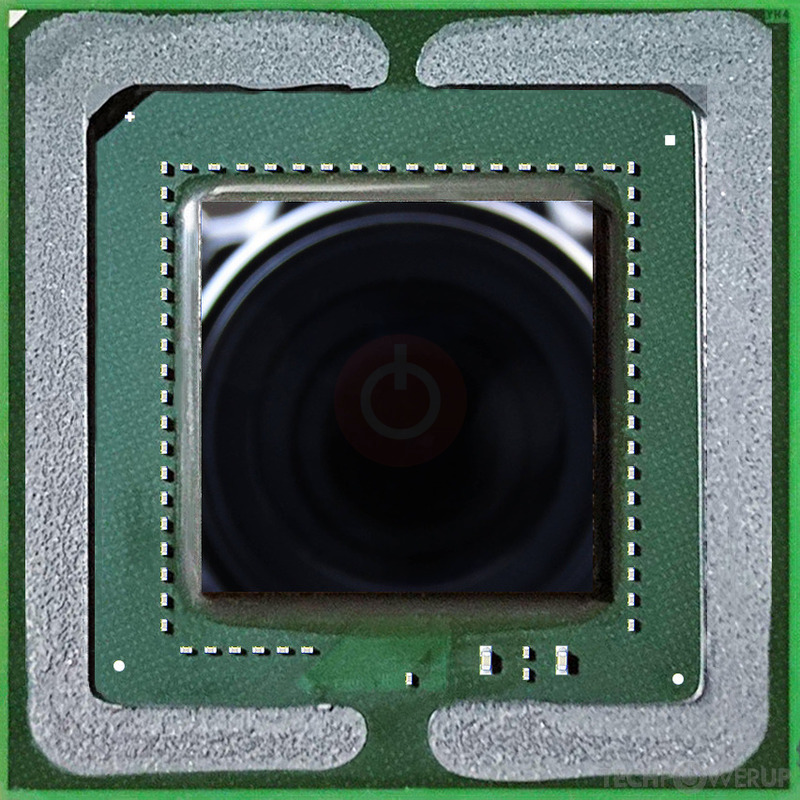
The Tesla S1075 was a professional graphics card by NVIDIA, launched on June 1st, 2008. Built on the 55 nm process, and based on the GT200B graphics processor, the card supports DirectX 11.1. Even though it supports DirectX 11, the feature level is only 10_0, which can be problematic with many DirectX 11 & DirectX 12 titles. The GT200B graphics processor is a large chip with a die area of 470 mm² and 1,400 million transistors. Tesla S1075 combines four graphics processors to increase performance. It features 240 shading units, 80 texture mapping units, and 32 ROPs, per GPU. NVIDIA has paired 16 GB GDDR3 memory with the Tesla S1075, which are connected using a 512-bit memory interface per GPU (each GPU manages 4,096 MB). The GPU is operating at a frequency of 610 MHz, memory is running at 800 MHz.
Being a dual-slot card, its power draw is rated at 800 W maximum. This device has no display connectivity, as it is not designed to have monitors connected to it. Tesla S1075 is connected to the rest of the system using a PCI-Express 2.0 x16 interface.
Being a dual-slot card, its power draw is rated at 800 W maximum. This device has no display connectivity, as it is not designed to have monitors connected to it. Tesla S1075 is connected to the rest of the system using a PCI-Express 2.0 x16 interface.
Graphics Processor
Graphics Card
- Release Date
- Jun 1st, 2008
- Generation
-
Tesla
(x10xx)
- Successor
- Tesla Fermi
- Production
- End-of-life
- Bus Interface
- PCIe 2.0 x16
Relative Performance
Based on TPU review data: "Performance Summary" at 1920x1080, 4K for 2080 Ti and faster.
Performance estimated based on architecture, shader count and clocks.
Clock Speeds
- GPU Clock
- 610 MHz
- Shader Clock
- 1296 MHz
- Memory Clock
-
800 MHz
1600 Mbps effective
Memory
- Memory Size
- 4 GB
- Memory Type
- GDDR3
- Memory Bus
- 512 bit
- Bandwidth
- 102.4 GB/s
Render Config
- Shading Units
- 240
- TMUs
- 80
- ROPs
- 32
- SM Count
- 30
- L2 Cache
- 256 KB
Theoretical Performance
- Pixel Rate
- 19.52 GPixel/s
- Texture Rate
- 48.80 GTexel/s
- FP32 (float)
- 622.1 GFLOPS
- FP64 (double)
- 77.76 GFLOPS (1:8)
Board Design
- Slot Width
- Dual-slot
- TDP
- 800 W
- Suggested PSU
- 1200 W
- Outputs
- No outputs
Graphics Features
- DirectX
- 11.1 (10_0)
- OpenGL
- 3.3
- OpenCL
- 1.1
- Vulkan
- N/A
- CUDA
- 1.3
- Shader Model
- 4.0
GT200B GPU Notes
| PureVideo HD: VP2 VDPAU: Feature Set A GT200B, commonly printed on the chip package as G200-xxx-Bx is an optical shrink of the G200 core to the newer 55 manufacturing process of TSMC. It helped shrink the core's energy and thermal footprints to a level that even facilitated building a dual-GPU accelerator |
Apr 27th, 2024 00:55 EDT
change timezone
Latest GPU Drivers
New Forum Posts
- What phone you use as your daily driver? And, a discussion of them. (1495)
- Strange system crashes out of nowhere, help (13)
- RX 580 VBIOS related functionality not supported for Device: 0x67df (9)
- Alphacool CORE 1 CPU block - bulging with danger of splitting? (33)
- hacked (78)
- 5800x (and other Zen 3 chips) PBO settings/Temperature fix (937)
- Is this a hardware problem ? Live kernel 193 (0)
- Help me to OC my 5700X (11)
- Realtek Modded Audio Driver for Windows 10/11 - Only for HDAUDIO (5690)
- What's your latest tech purchase? (20355)
Popular Reviews
- Ugreen NASync DXP4800 Plus Review
- HYTE THICC Q60 240 mm AIO Review
- MOONDROP x Crinacle DUSK In-Ear Monitors Review - The Last 5%
- Upcoming Hardware Launches 2023 (Updated Feb 2024)
- Quick Look: MOONDROP CHU 2 Budget In-Ear Monitors
- Thermalright Phantom Spirit 120 EVO Review
- FiiO K19 Desktop DAC/Headphone Amplifier Review
- Alienware Pro Wireless Gaming Keyboard Review
- AMD Ryzen 7 7800X3D Review - The Best Gaming CPU
- Corsair iCUE Link XC7 RGB Elite CPU Water Block Review
Controversial News Posts
- Windows 11 Now Officially Adware as Microsoft Embeds Ads in the Start Menu (135)
- Sony PlayStation 5 Pro Specifications Confirmed, Console Arrives Before Holidays (117)
- NVIDIA Points Intel Raptor Lake CPU Users to Get Help from Intel Amid System Instability Issues (106)
- AMD "Strix Halo" Zen 5 Mobile Processor Pictured: Chiplet-based, Uses 256-bit LPDDR5X (103)
- US Government Wants Nuclear Plants to Offload AI Data Center Expansion (98)
- AMD's RDNA 4 GPUs Could Stick with 18 Gbps GDDR6 Memory (95)
- Developers of Outpost Infinity Siege Recommend Underclocking i9-13900K and i9-14900K for Stability on Machines with RTX 4090 (85)
- Windows 10 Security Updates to Cost $61 After 2025, $427 by 2028 (84)