Report an Error


NVIDIA Quadro K4000
- Graphics Processor
- GK106
- Cores
- 768
- TMUs
- 64
- ROPs
- 24
- Memory Size
- 3 GB
- Memory Type
- GDDR5
- Bus Width
- 192 bit


GPU

I/O

Top
Bottom
Recommended Gaming Resolutions:
- 1600x900
- 1920x1080
- 2560x1440
The Quadro K4000 was an enthusiast-class professional graphics card by NVIDIA, launched on March 1st, 2013. Built on the 28 nm process, and based on the GK106 graphics processor, in its GK106-875-A1 variant, the card supports DirectX 12. The GK106 graphics processor is an average sized chip with a die area of 221 mm² and 2,540 million transistors. Unlike the fully unlocked GeForce GTX 660, which uses the same GPU but has all 960 shaders enabled, NVIDIA has disabled some shading units on the Quadro K4000 to reach the product's target shader count. It features 768 shading units, 64 texture mapping units, and 24 ROPs. NVIDIA has paired 3,072 MB GDDR5 memory with the Quadro K4000, which are connected using a 192-bit memory interface. The GPU is operating at a frequency of 810 MHz, memory is running at 1404 MHz (5.6 Gbps effective).
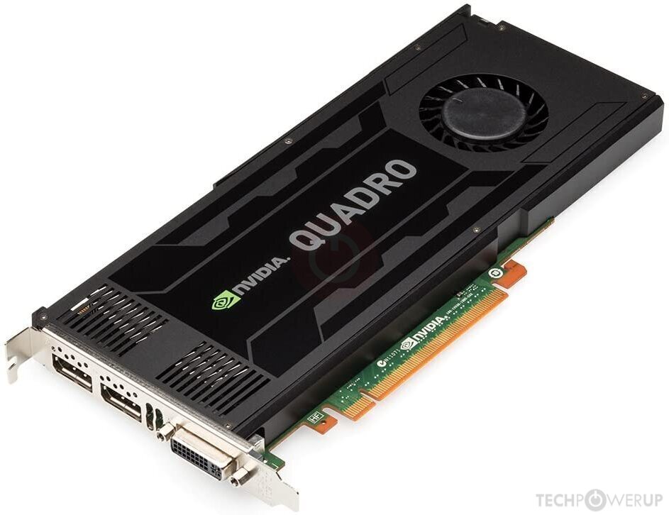
Being a single-slot card, the NVIDIA Quadro K4000 draws power from 1x 6-pin power connector, with power draw rated at 80 W maximum. Display outputs include: 1x DVI, 2x DisplayPort 1.2. Quadro K4000 is connected to the rest of the system using a PCI-Express 2.0 x16 interface. The card measures 241 mm in length, 111 mm in width, and features a single-slot cooling solution. Its price at launch was 1269 US Dollars.
Being a single-slot card, the NVIDIA Quadro K4000 draws power from 1x 6-pin power connector, with power draw rated at 80 W maximum. Display outputs include: 1x DVI, 2x DisplayPort 1.2. Quadro K4000 is connected to the rest of the system using a PCI-Express 2.0 x16 interface. The card measures 241 mm in length, 111 mm in width, and features a single-slot cooling solution. Its price at launch was 1269 US Dollars.
Graphics Processor
Graphics Card
- Release Date
- Mar 1st, 2013
- Generation
-
Quadro Kepler
(Kx000)
- Predecessor
- Quadro Fermi
- Successor
- Quadro Maxwell
- Production
- End-of-life
- Launch Price
- 1,269 USD
- Bus Interface
- PCIe 2.0 x16
- Reviews
- 26 in our database
Relative Performance
Based on TPU review data: "Performance Summary" at 1920x1080, 4K for 2080 Ti and faster.
Performance estimated based on architecture, shader count and clocks.
Clock Speeds
- GPU Clock
- 810 MHz
- Memory Clock
-
1404 MHz
5.6 Gbps effective
Memory
- Memory Size
- 3 GB
- Memory Type
- GDDR5
- Memory Bus
- 192 bit
- Bandwidth
- 134.8 GB/s
Render Config
- Shading Units
- 768
- TMUs
- 64
- ROPs
- 24
- SMX Count
- 4
- L1 Cache
- 16 KB (per SMX)
- L2 Cache
- 384 KB
Theoretical Performance
- Pixel Rate
- 12.96 GPixel/s
- Texture Rate
- 51.84 GTexel/s
- FP32 (float)
- 1,244 GFLOPS
- FP64 (double)
- 51.84 GFLOPS (1:24)
Board Design
- Slot Width
- Single-slot
- Length
- 241 mm
9.5 inches
- Width
- 111 mm
4.4 inches
- TDP
- 80 W
- Suggested PSU
- 250 W
- Outputs
- 1x DVI
2x DisplayPort 1.2
- Power Connectors
- 1x 6-pin
- Board Number
- P2030 SKU 500
Graphics Features
- DirectX
- 12 (11_0)
- OpenGL
- 4.6
- OpenCL
- 3.0
- Vulkan
- 1.2.175
- CUDA
- 3.0
- Shader Model
- 6.5 (5.1)
GK106 GPU Notes
| NVENC: 1st Gen NVDEC: 1st Gen PureVideo HD: VP5 VDPAU: Feature Set D L1 Cache is configurable from 16 KB up to 48 KB per SMX |
Apr 26th, 2024 04:55 EDT
change timezone
Latest GPU Drivers
New Forum Posts
- Horizontal black lines popping up on my screen? (7)
- What's your latest tech purchase? (20343)
- TPU's Nostalgic Hardware Club (18471)
- What are you playing? (20531)
- Which new games will you be buying? (320)
- Alphacool CORE 1 CPU block - bulging with danger of splitting? (21)
- Best SSD for system drive (82)
- What phone you use as your daily driver? And, a discussion of them. (1484)
- AMD RX 7000 series GPU Owners' Club (1087)
- im new to throttelstop and i think i messed it up by copying others any hints would be very much aprreciated (3)
Popular Reviews
- Fractal Design Terra Review
- Thermalright Phantom Spirit 120 EVO Review
- Corsair 2000D Airflow Review
- ASUS GeForce RTX 4090 STRIX OC Review
- NVIDIA GeForce RTX 4090 Founders Edition Review - Impressive Performance
- ASUS GeForce RTX 4090 Matrix Platinum Review - The RTX 4090 Ti
- MSI GeForce RTX 4090 Suprim X Review
- Gigabyte GeForce RTX 4090 Gaming OC Review
- MSI GeForce RTX 4090 Gaming X Trio Review
- MSI GeForce RTX 4090 Suprim Liquid X Review
Controversial News Posts
- Windows 11 Now Officially Adware as Microsoft Embeds Ads in the Start Menu (121)
- Sony PlayStation 5 Pro Specifications Confirmed, Console Arrives Before Holidays (117)
- NVIDIA Points Intel Raptor Lake CPU Users to Get Help from Intel Amid System Instability Issues (106)
- AMD "Strix Halo" Zen 5 Mobile Processor Pictured: Chiplet-based, Uses 256-bit LPDDR5X (101)
- US Government Wants Nuclear Plants to Offload AI Data Center Expansion (98)
- AMD's RDNA 4 GPUs Could Stick with 18 Gbps GDDR6 Memory (89)
- Developers of Outpost Infinity Siege Recommend Underclocking i9-13900K and i9-14900K for Stability on Machines with RTX 4090 (85)
- Windows 10 Security Updates to Cost $61 After 2025, $427 by 2028 (84)