Report an Error


NVIDIA GeForce GTX 770
- Graphics Processor
- GK104
- Cores
- 1536
- TMUs
- 128
- ROPs
- 32
- Memory Size
- 2 GB
- Memory Type
- GDDR5
- Bus Width
- 256 bit


GPU
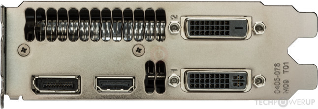
I/O

Top

Bottom

PCB Front
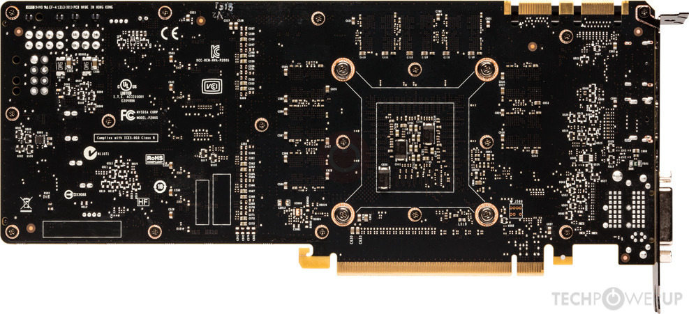
PCB Back
Recommended Gaming Resolutions:
- 1600x900
- 1920x1080
- 2560x1440
The GeForce GTX 770 was a high-end graphics card by NVIDIA, launched on May 30th, 2013. Built on the 28 nm process, and based on the GK104 graphics processor, in its GK104-425-A2 variant, the card supports DirectX 12. Even though it supports DirectX 12, the feature level is only 11_0, which can be problematic with newer DirectX 12 titles. The GK104 graphics processor is an average sized chip with a die area of 294 mm² and 3,540 million transistors. It features 1536 shading units, 128 texture mapping units, and 32 ROPs. NVIDIA has paired 2,048 MB GDDR5 memory with the GeForce GTX 770, which are connected using a 256-bit memory interface. The GPU is operating at a frequency of 1046 MHz, which can be boosted up to 1085 MHz, memory is running at 1753 MHz (7 Gbps effective).
Being a dual-slot card, the NVIDIA GeForce GTX 770 draws power from 1x 6-pin + 1x 8-pin power connector, with power draw rated at 230 W maximum. Display outputs include: 2x DVI, 1x HDMI 1.4a, 1x DisplayPort 1.2. GeForce GTX 770 is connected to the rest of the system using a PCI-Express 3.0 x16 interface. The card's dimensions are 267 mm x 111 mm x 38 mm, and it features a dual-slot cooling solution. Its price at launch was 399 US Dollars.
Being a dual-slot card, the NVIDIA GeForce GTX 770 draws power from 1x 6-pin + 1x 8-pin power connector, with power draw rated at 230 W maximum. Display outputs include: 2x DVI, 1x HDMI 1.4a, 1x DisplayPort 1.2. GeForce GTX 770 is connected to the rest of the system using a PCI-Express 3.0 x16 interface. The card's dimensions are 267 mm x 111 mm x 38 mm, and it features a dual-slot cooling solution. Its price at launch was 399 US Dollars.
Graphics Processor
Graphics Card
- Release Date
- May 30th, 2013
- Generation
- GeForce 700
- Predecessor
- GeForce 600
- Successor
- GeForce 900
- Production
- End-of-life
- Launch Price
- 399 USD
- Bus Interface
- PCIe 3.0 x16
- Reviews
- 112 in our database
Relative Performance
Based on TPU review data: "Performance Summary" at 1920x1080, 4K for 2080 Ti and faster.
Clock Speeds
- Base Clock
- 1046 MHz
- Boost Clock
- 1085 MHz
- Memory Clock
-
1753 MHz
7 Gbps effective
Memory
- Memory Size
- 2 GB
- Memory Type
- GDDR5
- Memory Bus
- 256 bit
- Bandwidth
- 224.4 GB/s
Render Config
- Shading Units
- 1536
- TMUs
- 128
- ROPs
- 32
- SMX Count
- 8
- L1 Cache
- 16 KB (per SMX)
- L2 Cache
- 512 KB
Theoretical Performance
- Pixel Rate
- 34.72 GPixel/s
- Texture Rate
- 138.9 GTexel/s
- FP32 (float)
- 3.333 TFLOPS
- FP64 (double)
- 138.9 GFLOPS (1:24)
Board Design
- Slot Width
- Dual-slot
- Length
- 267 mm
10.5 inches
- Width
- 111 mm
4.4 inches
- Height
- 38 mm
1.5 inches
- TDP
- 230 W
- Suggested PSU
- 550 W
- Outputs
- 2x DVI
1x HDMI 1.4a
1x DisplayPort 1.2
- Power Connectors
- 1x 6-pin + 1x 8-pin
- Board Number
- P2005 SKU 0
Graphics Features
- DirectX
- 12 (11_0)
- OpenGL
- 4.6
- OpenCL
- 3.0
- Vulkan
- 1.2.175
- CUDA
- 3.0
- Shader Model
- 6.5 (5.1)
GK104 GPU Notes
| NVENC: 1st Gen NVDEC: 1st Gen PureVideo HD: VP5 VDPAU: Feature Set D L1 Cache is configurable from 16 KB up to 48 KB per SMX |
Retail boards based on this design (84)
| Name | GPU Clock | Boost Clock | Memory Clock | Other Changes |
|---|---|---|---|---|
| 1058 MHz | 1110 MHz | 1753 MHz | 256 mm/10.1 inches | |
| 1046 MHz | 1085 MHz | 1753 MHz | 272 mm/10.7 inches | |
| 1046 MHz | 1085 MHz | 1753 MHz | 4 GB, 272 mm/10.7 inches | |
| 1058 MHz | 1110 MHz | 1753 MHz | 272 mm/10.7 inches | |
| 1058 MHz | 1110 MHz | 1753 MHz | 4 GB, 272 mm/10.7 inches | |
| 1165 MHz | 1215 MHz | 1753 MHz | ||
| 1110 MHz | 1163 MHz | 1753 MHz | ||
| 1176 MHz | 1229 MHz | 1800 MHz | ||
| 1163 MHz | 1202 MHz | 1820 MHz | 4 GB, 254 mm/10 inches | |
| 1070 MHz | 1100 MHz | 1753 MHz | ||
| 1070 MHz | 1100 MHz | 1753 MHz | 4 GB | |
| 1046 MHz | 1085 MHz | 1753 MHz | ||
| 1165 MHz | 1215 MHz | 1753 MHz | 4 GB, 279 mm/11 inches | |
| 1150 MHz | 1202 MHz | 1753 MHz | 4 GB | |
| 1150 MHz | 1202 MHz | 1753 MHz | 4 GB | |
| 1137 MHz | 1189 MHz | 1753 MHz | 4 GB | |
| 1110 MHz | 1163 MHz | 1753 MHz | ||
| 1110 MHz | 1163 MHz | 1753 MHz | 4 GB | |
| 1046 MHz | 1085 MHz | 1753 MHz | 4 GB | |
| 1085 MHz | 1137 MHz | 1753 MHz | ||
| 1085 MHz | 1137 MHz | 1753 MHz | ||
| 1110 MHz | 1163 MHz | 1753 MHz | ||
| 1085 MHz | 1137 MHz | 1753 MHz | ||
| 1046 MHz | 1085 MHz | 1753 MHz | ||
| 1046 MHz | 1085 MHz | 1753 MHz | ||
| 1046 MHz | 1085 MHz | 1753 MHz | 4 GB | |
| 1046 MHz | 1085 MHz | 1753 MHz | 280 mm/11 inches | |
| 1085 MHz | 1137 MHz | 1753 MHz | 280 mm/11 inches | |
| 1150 MHz | 1202 MHz | 1753 MHz | 274 mm/10.8 inches | |
| 1046 MHz | 1085 MHz | 1753 MHz | 4 GB | |
| 1110 MHz | 1163 MHz | 1753 MHz | 268 mm/10.6 inches | |
| 1110 MHz | 1163 MHz | 1753 MHz | 4 GB, 268 mm/10.6 inches | |
| 1202 MHz | 1254 MHz | 1753 MHz | 289 mm/11.4 inches, 1x DisplayPort 3x mini-HDMI | |
| 1150 MHz | 1202 MHz | 1753 MHz | 289 mm/11.4 inches, 1x DisplayPort 3x mini-HDMI | |
| 1046 MHz | 1085 MHz | 1753 MHz | 292 mm/11.5 inches | |
| 1046 MHz | 1085 MHz | 1753 MHz | 4 GB, 292 mm/11.5 inches | |
| 1046 MHz | 1085 MHz | 1753 MHz | 4 GB, 292 mm/11.5 inches | |
| 1137 MHz | 1189 MHz | 1753 MHz | 292 mm/11.5 inches | |
| 1137 MHz | 1189 MHz | 1753 MHz | 4 GB, 292 mm/11.5 inches | |
| 1137 MHz | 1189 MHz | 1753 MHz | 4 GB, 292 mm/11.5 inches | |
| 1110 MHz | 1163 MHz | 1753 MHz | 255 mm/10 inches | |
| 1046 MHz | 1085 MHz | 1753 MHz | ||
| 1072 MHz | 1110 MHz | 1753 MHz | 255 mm/10 inches | |
| 1072 MHz | 1110 MHz | 1753 MHz | 4 GB, 255 mm/10 inches | |
| 1163 MHz | 1215 MHz | 1820 MHz | ||
| 1163 MHz | 1215 MHz | 1820 MHz | 4 GB | |
| 1150 MHz | 1202 MHz | 1800 MHz | 288 mm/11.3 inches | |
| 1150 MHz | 1202 MHz | 1800 MHz | 4 GB, 288 mm/11.3 inches | |
| 1110 MHz | 1163 MHz | 1753 MHz | 268 mm/10.6 inches | |
| 1202 MHz | 1254 MHz | 1753 MHz | ||
| 1058 MHz | 1110 MHz | 1753 MHz | 270 mm/10.6 inches | |
| 1058 MHz | 1110 MHz | 1753 MHz | 4 GB, 270 mm/10.6 inches | |
| 1046 MHz | 1085 MHz | 1753 MHz | 280 mm/11 inches | |
| 1150 MHz | 1202 MHz | 1753 MHz | 280 mm/11 inches | |
| 1046 MHz | 1085 MHz | 1753 MHz | 4 GB, 272 mm/10.7 inches | |
| 1046 MHz | 1085 MHz | 1753 MHz | 268 mm/10.6 inches | |
| 1058 MHz | 1110 MHz | 1753 MHz | 260 mm/10.2 inches | |
| 1072 MHz | 1124 MHz | 1753 MHz | 4 GB, 260 mm/10.2 inches | |
| 1085 MHz | 1137 MHz | 1753 MHz | 260 mm/10.2 inches | |
| 1137 MHz | 1189 MHz | 1753 MHz | 4 GB, 260 mm/10.2 inches | |
| 1150 MHz | 1202 MHz | 1753 MHz | 280 mm/11 inches | |
| 1072 MHz | 1124 MHz | 1753 MHz | 268 mm/10.6 inches | |
| 1046 MHz | 1085 MHz | 1753 MHz | ||
| 1046 MHz | 1085 MHz | 1753 MHz | 280 mm/11 inches | |
| 1150 MHz | 1202 MHz | 1753 MHz | 280 mm/11 inches | |
| 1046 MHz | 1085 MHz | 1753 MHz | 4 GB, 272 mm/10.7 inches | |
| 1085 MHz | 1137 MHz | 1753 MHz | 280 mm/11 inches | |
| 1046 MHz | 1085 MHz | 1753 MHz | 280 mm/11 inches | |
| 1046 MHz | 1085 MHz | 1753 MHz | 256 mm/10.1 inches | |
| 1150 MHz | 1202 MHz | 1800 MHz | 270 mm/10.6 inches | |
| 1058 MHz | 1110 MHz | 1753 MHz | 4 GB, 270 mm/10.6 inches | |
| 1150 MHz | 1202 MHz | 1753 MHz | 4 GB, 270 mm/10.6 inches | |
| 1058 MHz | 1110 MHz | 1750 MHz | 270 mm/10.6 inches | |
| 1150 MHz | 1202 MHz | 1800 MHz | 270 mm/10.6 inches | |
| 1058 MHz | 1110 MHz | 1753 MHz | ||
| 1150 MHz | 1202 MHz | 1753 MHz | 280 mm/11 inches | |
| 1046 MHz | 1085 MHz | 1753 MHz | 4 GB, 272 mm/10.7 inches | |
| 1058 MHz | 1110 MHz | 1753 MHz | 256 mm/10.1 inches | |
| 1150 MHz | 1202 MHz | 1800 MHz | ||
| 1150 MHz | 1202 MHz | 1753 MHz | 4 GB | |
| 1058 MHz | 1110 MHz | 1753 MHz | ||
| 1058 MHz | 1110 MHz | 1753 MHz | 4 GB | |
| 1150 MHz | 1202 MHz | 1800 MHz | ||
| 1150 MHz | 1202 MHz | 1800 MHz |


Apr 26th, 2024 17:57 EDT
change timezone
Latest GPU Drivers
New Forum Posts
- looking to build a new system and im considering asrock brand but i have some doubts/concerns. (5)
- TPU's Nostalgic Hardware Club (18474)
- What's your latest tech purchase? (20354)
- 5800x (and other Zen 3 chips) PBO settings/Temperature fix (934)
- Only EDP Other in Core? (2)
- Alphacool CORE 1 CPU block - bulging with danger of splitting? (30)
- Dell Workstation Owners Club (3061)
- Xeon Owners Club (8700)
- Secure boot already open help (10)
- hacked (77)
Popular Reviews
- HYTE THICC Q60 240 mm AIO Review
- MOONDROP x Crinacle DUSK In-Ear Monitors Review - The Last 5%
- Upcoming Hardware Launches 2023 (Updated Feb 2024)
- Alienware Pro Wireless Gaming Keyboard Review
- Thermalright Phantom Spirit 120 EVO Review
- FiiO K19 Desktop DAC/Headphone Amplifier Review
- ASUS Radeon RX 7900 GRE TUF OC Review
- Ugreen NASync DXP4800 Plus Review
- AMD Ryzen 7 7800X3D Review - The Best Gaming CPU
- Sapphire Radeon RX 7900 GRE Pulse Review
Controversial News Posts
- Windows 11 Now Officially Adware as Microsoft Embeds Ads in the Start Menu (135)
- Sony PlayStation 5 Pro Specifications Confirmed, Console Arrives Before Holidays (117)
- NVIDIA Points Intel Raptor Lake CPU Users to Get Help from Intel Amid System Instability Issues (106)
- AMD "Strix Halo" Zen 5 Mobile Processor Pictured: Chiplet-based, Uses 256-bit LPDDR5X (103)
- US Government Wants Nuclear Plants to Offload AI Data Center Expansion (98)
- AMD's RDNA 4 GPUs Could Stick with 18 Gbps GDDR6 Memory (95)
- Developers of Outpost Infinity Siege Recommend Underclocking i9-13900K and i9-14900K for Stability on Machines with RTX 4090 (85)
- Windows 10 Security Updates to Cost $61 After 2025, $427 by 2028 (84)