Report an Error


NVIDIA GeForce GTX 760 Ti OEM Rebrand
- Graphics Processor
- GK104
- Cores
- 1344
- TMUs
- 112
- ROPs
- 32
- Memory Size
- 2 GB
- Memory Type
- GDDR5
- Bus Width
- 256 bit

GPU

I/O

Top

Bottom
Recommended Gaming Resolutions:
- 1366x768
- 1600x900
- 1920x1080
The GeForce GTX 760 Ti OEM Rebrand was a graphics card by NVIDIA, launched on August 25th, 2013. Built on the 28 nm process, and based on the GK104 graphics processor, in its GK104-325-A2 variant, the card supports DirectX 12. Even though it supports DirectX 12, the feature level is only 11_0, which can be problematic with newer DirectX 12 titles. The GK104 graphics processor is an average sized chip with a die area of 294 mm² and 3,540 million transistors. Unlike the fully unlocked GeForce GTX 680, which uses the same GPU but has all 1536 shaders enabled, NVIDIA has disabled some shading units on the GeForce GTX 760 Ti OEM Rebrand to reach the product's target shader count. It features 1344 shading units, 112 texture mapping units, and 32 ROPs. NVIDIA has paired 2,048 MB GDDR5 memory with the GeForce GTX 760 Ti OEM Rebrand, which are connected using a 256-bit memory interface. The GPU is operating at a frequency of 915 MHz, which can be boosted up to 980 MHz, memory is running at 1502 MHz (6 Gbps effective).
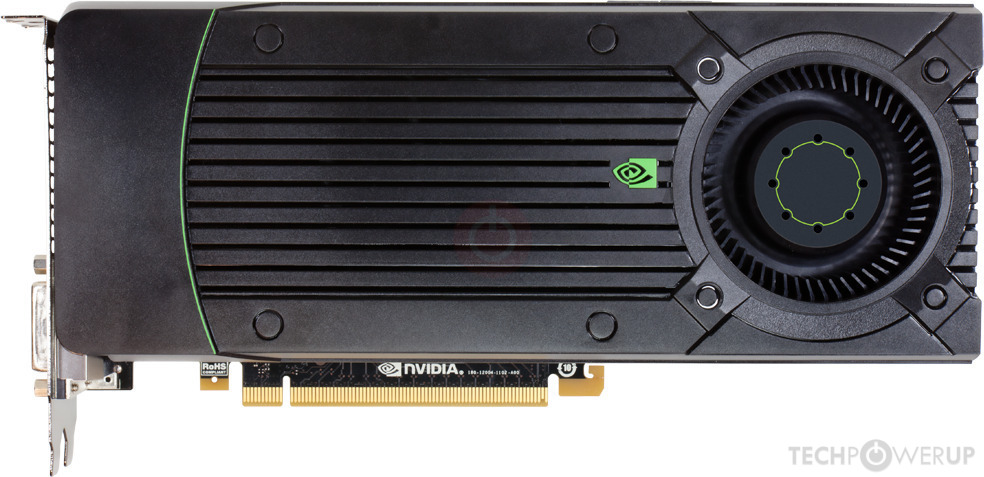
Being a dual-slot card, the NVIDIA GeForce GTX 760 Ti OEM Rebrand draws power from 2x 6-pin power connectors, with power draw rated at 170 W maximum. Display outputs include: 2x DVI, 1x HDMI 1.4a, 1x DisplayPort 1.2. GeForce GTX 760 Ti OEM Rebrand is connected to the rest of the system using a PCI-Express 3.0 x16 interface. The card measures 241 mm in length, and features a dual-slot cooling solution.
Being a dual-slot card, the NVIDIA GeForce GTX 760 Ti OEM Rebrand draws power from 2x 6-pin power connectors, with power draw rated at 170 W maximum. Display outputs include: 2x DVI, 1x HDMI 1.4a, 1x DisplayPort 1.2. GeForce GTX 760 Ti OEM Rebrand is connected to the rest of the system using a PCI-Express 3.0 x16 interface. The card measures 241 mm in length, and features a dual-slot cooling solution.
Graphics Processor
Graphics Card
- Release Date
- Aug 25th, 2013
- Generation
- GeForce 700
- Predecessor
- GeForce 600
- Successor
- GeForce 900
- Production
- End-of-life
- Bus Interface
- PCIe 3.0 x16
Relative Performance
Based on TPU review data: "Performance Summary" at 1920x1080, 4K for RTX 3080 and faster.
Performance estimated based on architecture, shader count and clocks.
Clock Speeds
- Base Clock
- 915 MHz
- Boost Clock
- 980 MHz
- Memory Clock
-
1502 MHz
6 Gbps effective
Memory
- Memory Size
- 2 GB
- Memory Type
- GDDR5
- Memory Bus
- 256 bit
- Bandwidth
- 192.3 GB/s
Render Config
- Shading Units
- 1344
- TMUs
- 112
- ROPs
- 32
- SMX Count
- 7
- L1 Cache
- 16 KB (per SMX)
- L2 Cache
- 512 KB
Theoretical Performance
- Pixel Rate
- 27.44 GPixel/s
- Texture Rate
- 109.8 GTexel/s
- FP32 (float)
- 2.634 TFLOPS
- FP64 (double)
- 109.8 GFLOPS (1:24)
Board Design
- Slot Width
- Dual-slot
- Length
- 241 mm
9.5 inches
- TDP
- 170 W
- Suggested PSU
- 450 W
- Outputs
- 2x DVI
1x HDMI 1.4a
1x DisplayPort 1.2
- Power Connectors
- 2x 6-pin
- Board Number
- P2004 SKU 5
Graphics Features
- DirectX
- 12 (11_0)
- OpenGL
- 4.6
- OpenCL
- 3.0
- Vulkan
- 1.2.175
- CUDA
- 3.0
- Shader Model
- 6.5 (5.1)
Card Notes
| Rebranded GTX 670 |
GK104 GPU Notes
| NVENC: 1st Gen NVDEC: 1st Gen PureVideo HD: VP5 VDPAU: Feature Set D L1 Cache is configurable from 16 KB up to 48 KB per SMX Latest Drivers: Windows XP / Server 2003 x64: Quadro Release R319 U2 (321.01) Windows Vista: GeForce Release 365.19 Quadro Release R346 U7 (348.40) / R352 BETA (352.86) Windows 7 / 8 / 8.1 / 10 / 11 (x32 / x64): GeForce Release 391.35 / 475.06 Quadro Release R390 U9 (392.37) / R470 U16 (474.82) Data Center Release 427.11 Tesla Release 441.22 Windows 10 / 11 x64: GeForce Release 475.06 Quadro Release R470 U16 (474.82) Data Center Release 474.82 |
Jul 24th, 2025 15:29 CDT
change timezone
Latest GPU Drivers
New Forum Posts
- Share your CPUZ Benchmarks! (2533)
- What are these keycaps? (1)
- AI Job Losses: let's count the losses up, total losses to AI so far 94,000 and counting (59)
- RX 9000 series GPU Owners Club (1192)
- Need some help finding correct VBIOS for my RX580 (8)
- What's your latest tech purchase? (24356)
- 14900k high voltage (42)
- Corsair RM850x (2021) 12V Rail Dropping — Causing Crashes While Gaming (0)
- GTX 1660ti GALAX OC UEFI BIOS (0)
- Budget friendly upgrading from 970? (0)
Popular Reviews
- Noctua NF-A12x25 G2 PWM Fan Review
- MSI MPG B850I Edge Ti Wi-Fi Review
- Cougar OmnyX Review
- Thermal Grizzly WireView Pro Review
- UPERFECT UMax 24 Review
- TerraMaster F4-424 Max Review - The fastest NAS we've tested so far
- Sharkoon OfficePal C10 Review - Affordable and Decent
- Razer Blade 16 (2025) Review - Thin, Light, Punchy, and Efficient
- Upcoming Hardware Launches 2025 (Updated May 2025)
- VAXEE XE V2 Wireless Review
TPU on YouTube
Controversial News Posts
- Some Intel Nova Lake CPUs Rumored to Challenge AMD's 3D V-Cache in Desktop Gaming (140)
- AMD Radeon RX 9070 XT Gains 9% Performance at 1440p with Latest Driver, Beats RTX 5070 Ti (131)
- AMD's Upcoming UDNA / RDNA 5 GPU Could Feature 96 CUs and 384-bit Memory Bus (116)
- NVIDIA GeForce RTX 5080 SUPER Could Feature 24 GB Memory, Increased Power Limits (115)
- NVIDIA DLSS Transformer Cuts VRAM Usage by 20% (99)
- AMD Sampling Next-Gen Ryzen Desktop "Medusa Ridge," Sees Incremental IPC Upgrade, New cIOD (97)
- NVIDIA Becomes First Company Ever to Hit $4 Trillion Market-Cap (94)
- Windows 12 Delayed as Microsoft Prepares Windows 11 25H2 Update (92)