Report an Error


NVIDIA GeForce GT 440 OEM
- Graphics Processor
- GF106
- Cores
- 144
- TMUs
- 24
- ROPs
- 24
- Memory Size
- 1536 MB
- Memory Type
- DDR3
- Bus Width
- 192 bit
GPU
I/O
Recommended Gaming Resolutions:
- 1280x720
- 1366x768
- 1600x900
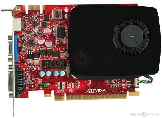
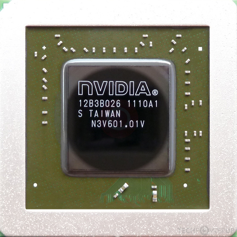
The GeForce GT 440 OEM was a graphics card by NVIDIA, launched on October 11th, 2010. Built on the 40 nm process, and based on the GF106 graphics processor, the card supports DirectX 12. Even though it supports DirectX 12, the feature level is only 11_0, which can be problematic with newer DirectX 12 titles. The GF106 graphics processor is an average sized chip with a die area of 238 mm² and 1,170 million transistors. Unlike the fully unlocked GeForce GTS 450, which uses the same GPU but has all 192 shaders enabled, NVIDIA has disabled some shading units on the GeForce GT 440 OEM to reach the product's target shader count. It features 144 shading units, 24 texture mapping units, and 24 ROPs. NVIDIA has paired 1,536 MB DDR3 memory with the GeForce GT 440 OEM, which are connected using a 192-bit memory interface. The GPU is operating at a frequency of 810 MHz, memory is running at 900 MHz.
Being a single-slot card, the NVIDIA GeForce GT 440 OEM does not require any additional power connector, its power draw is rated at 65 W maximum. Display outputs include: 1x DVI, 1x HDMI 1.3a, 1x VGA. GeForce GT 440 OEM is connected to the rest of the system using a PCI-Express 2.0 x16 interface. The card measures 145 mm in length, and features a single-slot cooling solution.
Being a single-slot card, the NVIDIA GeForce GT 440 OEM does not require any additional power connector, its power draw is rated at 65 W maximum. Display outputs include: 1x DVI, 1x HDMI 1.3a, 1x VGA. GeForce GT 440 OEM is connected to the rest of the system using a PCI-Express 2.0 x16 interface. The card measures 145 mm in length, and features a single-slot cooling solution.
Graphics Processor
Graphics Card
- Release Date
- Oct 11th, 2010
- Generation
- GeForce 400
- Predecessor
- GeForce 200
- Successor
- GeForce 500
- Production
- End-of-life
- Bus Interface
- PCIe 2.0 x16
- Reviews
- 5 in our database
Relative Performance
Based on TPU review data: "Performance Summary" at 1920x1080, 4K for 2080 Ti and faster.
Performance estimated based on architecture, shader count and clocks.
Clock Speeds
- GPU Clock
- 810 MHz
- Shader Clock
- 1620 MHz
- Memory Clock
-
900 MHz
1800 Mbps effective
Memory
- Memory Size
- 1536 MB
- Memory Type
- DDR3
- Memory Bus
- 192 bit
- Bandwidth
- 43.20 GB/s
Render Config
- Shading Units
- 144
- TMUs
- 24
- ROPs
- 24
- SM Count
- 3
- L1 Cache
- 64 KB (per SM)
- L2 Cache
- 384 KB
Theoretical Performance
- Pixel Rate
- 4.860 GPixel/s
- Texture Rate
- 19.44 GTexel/s
- FP32 (float)
- 466.6 GFLOPS
- FP64 (double)
- 38.88 GFLOPS (1:12)
Board Design
- Slot Width
- Single-slot
- Length
- 145 mm
5.7 inches
- TDP
- 65 W
- Suggested PSU
- 250 W
- Outputs
- 1x DVI
1x HDMI 1.3a
1x VGA
- Power Connectors
- None
- Board Number
- P1062 SKU 1
Graphics Features
- DirectX
- 12 (11_0)
- OpenGL
- 4.6
- OpenCL
- 1.1
- Vulkan
- N/A
- CUDA
- 2.1
- Shader Model
- 5.1
GF106 GPU Notes
| PureVideo HD: VP4 VDPAU: Feature Set C |
May 13th, 2024 17:03 EDT
change timezone
Latest GPU Drivers
New Forum Posts
- Keyboard cleaning crime (23)
- Which RAM for AMD 7950X3D (7)
- macOS Sonoma and USB hubs (0)
- Purchased an AX1200i PSU as part of some forward planning, what tier is this PSU? (92)
- LOWER SSD PRICES (20)
- Laptop i7 11800H Throttling Immediately (1)
- How can we utilize Artificial Intelligence to help us be more prescient about quality of life and environment? (45)
- Last game you purchased? (288)
- PKG Power much higher than usual (9)
- 2024 and STILL no dark mode? (44)
Popular Reviews
- ZMF Caldera Closed Planar Magnetic Headphones Review
- Homeworld 3 Performance Benchmark Review - 35 GPUs Tested
- Corsair MP700 Pro SE 4 TB Review
- Bykski CPU-XPR-C-I CPU Water Block Review - Amazing Value!
- ThundeRobot ML903 NearLink Review
- Upcoming Hardware Launches 2023 (Updated Feb 2024)
- AMD Ryzen 7 7800X3D Review - The Best Gaming CPU
- CHERRY XTRFY M64 Pro Review
- ASUS Radeon RX 7900 GRE TUF OC Review
- Corsair iCUE Link RX120 RGB 120 mm Fan Review
Controversial News Posts
- Intel Statement on Stability Issues: "Motherboard Makers to Blame" (266)
- AMD to Redesign Ray Tracing Hardware on RDNA 4 (226)
- Windows 11 Now Officially Adware as Microsoft Embeds Ads in the Start Menu (172)
- NVIDIA to Only Launch the Flagship GeForce RTX 5090 in 2024, Rest of the Series in 2025 (152)
- Sony PlayStation 5 Pro Specifications Confirmed, Console Arrives Before Holidays (119)
- AMD Hits Highest-Ever x86 CPU Market Share in Q1 2024 Across Desktop and Server (115)
- AMD's RDNA 4 GPUs Could Stick with 18 Gbps GDDR6 Memory (114)
- AMD Ryzen 9 7900X3D Now at a Mouth-watering $329 (104)