Report an Error

AMD Radeon R7 M340
- Graphics Processor
- Meso
- Cores
- 320
- TMUs
- 20
- ROPs
- 8
- Memory Size
- 2 GB
- Memory Type
- DDR3
- Bus Width
- 64 bit
GPU
Recommended Gaming Resolutions:
- 1366x768
- 1600x900
- 1920x1080
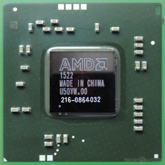
The Radeon R7 M340 was a mobile graphics chip by AMD, launched on May 5th, 2015. Built on the 28 nm process, and based on the Meso graphics processor, in its Meso PRO variant, the chip supports DirectX 12. This ensures that all modern games will run on Radeon R7 M340. The Meso graphics processor is an average sized chip with a die area of 125 mm² and 1,550 million transistors. Unlike the fully unlocked Radeon R7 A360, which uses the same GPU but has all 384 shaders enabled, AMD has disabled some shading units on the Radeon R7 M340 to reach the product's target shader count. It features 320 shading units, 20 texture mapping units, and 8 ROPs. AMD has paired 2,048 MB DDR3 memory with the Radeon R7 M340, which are connected using a 64-bit memory interface. The GPU is operating at a frequency of 943 MHz, which can be boosted up to 1021 MHz, memory is running at 1000 MHz.
Its power draw is not exactly known. This device has no display connectivity, as it is not designed to have monitors connected to it. Rather it is intended for use in laptop/notebooks and will use the output of the host mobile device. Radeon R7 M340 is connected to the rest of the system using a PCI-Express 3.0 x8 interface.
Its power draw is not exactly known. This device has no display connectivity, as it is not designed to have monitors connected to it. Rather it is intended for use in laptop/notebooks and will use the output of the host mobile device. Radeon R7 M340 is connected to the rest of the system using a PCI-Express 3.0 x8 interface.
Graphics Processor
Mobile Graphics
- Release Date
- May 5th, 2015
- Generation
-
Gem System
(R7 M300)
- Predecessor
- Solar System
- Successor
- Polaris Mobile
- Production
- End-of-life
- Bus Interface
- PCIe 3.0 x8
Relative Performance
Based on TPU review data: "Performance Summary" at 1920x1080, 4K for 2080 Ti and faster.
Performance estimated based on architecture, shader count and clocks.
Clock Speeds
- Base Clock
- 943 MHz
- Boost Clock
- 1021 MHz
- Memory Clock
-
1000 MHz
2 Gbps effective
Memory
- Memory Size
- 2 GB
- Memory Type
- DDR3
- Memory Bus
- 64 bit
- Bandwidth
- 16.00 GB/s
Render Config
- Shading Units
- 320
- TMUs
- 20
- ROPs
- 8
- Compute Units
- 5
- L1 Cache
- 16 KB (per CU)
- L2 Cache
- 128 KB
Theoretical Performance
- Pixel Rate
- 8.168 GPixel/s
- Texture Rate
- 20.42 GTexel/s
- FP16 (half)
- 653.4 GFLOPS (1:1)
- FP32 (float)
- 653.4 GFLOPS
- FP64 (double)
- 40.84 GFLOPS (1:16)
Board Design
- TDP
- unknown
- Outputs
- Portable Device Dependent
Graphics Features
- DirectX
- 12 (12_0)
- OpenGL
- 4.6
- OpenCL
- 2.1
- Vulkan
- 1.2.170
- Shader Model
- 6.5
Meso GPU Notes
| Generation: Volcanic Islands Desktop Variant: Iceland Mobile Variant: Topaz / Weston / Polaris 24 Graphics/Compute: GFX8 (gfx802) Display Core Engine: No Support Unified Video Decoder: No Support Video Compression Engine: No Support System DMA: 2.0.0 CLRX: GCN 1.2.0 |
Apr 26th, 2024 22:49 EDT
change timezone
Latest GPU Drivers
New Forum Posts
- Black screens leading to restarts (Event ID 18) on AMD platform since changing graphics card (43)
- FINAL FANTASY XIV: Dawntrail Official Benchmark (73)
- Your PC ATM (34509)
- Rare GPUs / Unreleased GPUs (1877)
- looking to build a new system and im considering asrock brand but i have some doubts/concerns. (15)
- AAF Optimus DCH Audio Modded Driver for Windows 10/11 - For ALL HDAUDIO Enumerator Chips (652)
- Help me identify rx 580 card ? (0)
- Strange system crashes out of nowhere help (9)
- What phone you use as your daily driver? And, a discussion of them. (1494)
- Secure boot already open help (11)
Popular Reviews
- Ugreen NASync DXP4800 Plus Review
- HYTE THICC Q60 240 mm AIO Review
- Quick Look: MOONDROP CHU 2 Budget In-Ear Monitors
- MOONDROP x Crinacle DUSK In-Ear Monitors Review - The Last 5%
- Thermalright Phantom Spirit 120 EVO Review
- Upcoming Hardware Launches 2023 (Updated Feb 2024)
- Alienware Pro Wireless Gaming Keyboard Review
- CeBIT 2008: Akasa Review
- CeBIT 2008: Cyber E Sport Review
- FiiO K19 Desktop DAC/Headphone Amplifier Review
Controversial News Posts
- Windows 11 Now Officially Adware as Microsoft Embeds Ads in the Start Menu (135)
- Sony PlayStation 5 Pro Specifications Confirmed, Console Arrives Before Holidays (117)
- NVIDIA Points Intel Raptor Lake CPU Users to Get Help from Intel Amid System Instability Issues (106)
- AMD "Strix Halo" Zen 5 Mobile Processor Pictured: Chiplet-based, Uses 256-bit LPDDR5X (103)
- US Government Wants Nuclear Plants to Offload AI Data Center Expansion (98)
- AMD's RDNA 4 GPUs Could Stick with 18 Gbps GDDR6 Memory (95)
- Developers of Outpost Infinity Siege Recommend Underclocking i9-13900K and i9-14900K for Stability on Machines with RTX 4090 (85)
- Windows 10 Security Updates to Cost $61 After 2025, $427 by 2028 (84)