Report an Error


NVIDIA GeForce GTX 980 Mobile
- Graphics Processor
- GM204
- Cores
- 2048
- TMUs
- 128
- ROPs
- 64
- Memory Size
- 8 GB
- Memory Type
- GDDR5
- Bus Width
- 256 bit

GPU
Recommended Gaming Resolutions:
- 1600x900
- 1920x1080
- 2560x1440
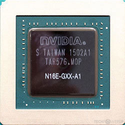
The GeForce GTX 980 Mobile was a mobile graphics chip by NVIDIA, launched on September 21st, 2015. Built on the 28 nm process, and based on the GM204 graphics processor, in its N16E-GXX-A1 variant, the chip supports DirectX 12. This ensures that all modern games will run on GeForce GTX 980 Mobile. The GM204 graphics processor is a large chip with a die area of 398 mm² and 5,200 million transistors. It features 2048 shading units, 128 texture mapping units, and 64 ROPs. NVIDIA has paired 8 GB GDDR5 memory with the GeForce GTX 980 Mobile, which are connected using a 256-bit memory interface. The GPU is operating at a frequency of 1064 MHz, which can be boosted up to 1140 MHz, memory is running at 1753 MHz (7 Gbps effective).
Being a mxm module card, the NVIDIA GeForce GTX 980 Mobile does not require any additional power connector, its power draw is not exactly known. This device has no display connectivity, as it is not designed to have monitors connected to it. Rather it is intended for use in laptop/notebooks and will use the output of the host mobile device.
Being a mxm module card, the NVIDIA GeForce GTX 980 Mobile does not require any additional power connector, its power draw is not exactly known. This device has no display connectivity, as it is not designed to have monitors connected to it. Rather it is intended for use in laptop/notebooks and will use the output of the host mobile device.
Graphics Processor
- GPU Name
- GM204
- GPU Variant
- N16E-GXX-A1
- Architecture
- Maxwell 2.0
- Foundry
- TSMC
- Process Size
- 28 nm
- Transistors
- 5,200 million
- Density
- 13.1M / mm²
- Die Size
- 398 mm²
- Chip Package
- BGA-1745
Mobile Graphics
- Release Date
- Sep 21st, 2015
- Generation
- GeForce 900M
- Predecessor
- GeForce 800M
- Successor
- GeForce 10 Mobile
- Production
- End-of-life
- Bus Interface
- MXM-B (3.0)
- Reviews
- 146 in our database
Relative Performance
Based on TPU review data: "Performance Summary" at 1920x1080, 4K for 2080 Ti and faster.
Performance estimated based on architecture, shader count and clocks.
Clock Speeds
- Base Clock
- 1064 MHz
- Boost Clock
- 1140 MHz
- Memory Clock
-
1753 MHz
7 Gbps effective
Memory
- Memory Size
- 8 GB
- Memory Type
- GDDR5
- Memory Bus
- 256 bit
- Bandwidth
- 224.4 GB/s
Render Config
- Shading Units
- 2048
- TMUs
- 128
- ROPs
- 64
- SMM Count
- 16
- L1 Cache
- 48 KB (per SMM)
- L2 Cache
- 2 MB
Theoretical Performance
- Pixel Rate
- 72.96 GPixel/s
- Texture Rate
- 145.9 GTexel/s
- FP32 (float)
- 4.669 TFLOPS
- FP64 (double)
- 145.9 GFLOPS (1:32)
Board Design
- Slot Width
- MXM Module
- TDP
- unknown
- Outputs
- Portable Device Dependent
- Power Connectors
- None
Graphics Features
- DirectX
- 12 (12_1)
- OpenGL
- 4.6
- OpenCL
- 3.0
- Vulkan
- 1.3
- CUDA
- 5.2
- Shader Model
- 6.8
GM204 GPU Notes
| NVENC: 5th Gen NVDEC: 1st Gen PureVideo HD: VP6 VDPAU: Feature Set E Latest Drivers: Windows Vista: GeForce Release 365.19 Quadro Release R346 U7 (348.40) / R352 BETA (352.86) Windows 7 / 8 / 8.1 (x32 / x64): GeForce Release 391.35 / 474.89 Quadro Release R390 U9 (392.37) / R440 U4 (441.66) Data Center Release 427.11 Windows 10 / 11 (x32 / x64): GeForce Release 391.35 / Latest Quadro Release R390 U9 (392.37) / Latest Data Center Release: Latest |
Devices based on this design (2)
| Name | GPU Clock | Boost Clock | Memory Clock | Other Changes |
|---|---|---|---|---|
| 1127 MHz | 1216 MHz | 1503 MHz | ||
| 1190 MHz | 1291 MHz | 1753 MHz | 4 GB |


Jun 28th, 2025 17:35 CDT
change timezone
Latest GPU Drivers
New Forum Posts
- Best time to sell your used 4090s is now. (257)
- Bitlocker doesnt auto-unlock ext drive (2)
- SLI is really not Dead if you Have a SLI rig (116)
- What air cooler should I get for Jonsbo Z20-9800X3D? (5)
- X79 and/or rampage IV OC'ing thread for those of us still left.... (2418)
- Page loading issues from Russia (50)
- Can anyone recomend a video course on basic computer repair? (39)
- Kingston WI-Drive 128GB looking ill today!! (14)
- The TPU UK Clubhouse (26503)
- Can you guess Which game it is? (187)
Popular Reviews
- ASRock Phantom Gaming Z890 Riptide Wi-Fi Review
- Sapphire Radeon RX 9060 XT Pulse OC 16 GB Review - Samsung Memory Tested
- SCHENKER KEY 18 Pro (E25) Review - Top-Tier Contender
- Lexar NQ780 4 TB Review
- AMD Ryzen 7 9800X3D Review - The Best Gaming Processor
- Upcoming Hardware Launches 2025 (Updated May 2025)
- AVerMedia CamStream 4K Review
- Sapphire Radeon RX 9070 XT Nitro+ Review - Beating NVIDIA
- NVIDIA GeForce RTX 5060 8 GB Review
- Intel Core Ultra 7 265K Review
TPU on YouTube
Controversial News Posts
- Intel's Core Ultra 7 265K and 265KF CPUs Dip Below $250 (287)
- NVIDIA Grabs Market Share, AMD Loses Ground, and Intel Disappears in Latest dGPU Update (204)
- Microsoft Partners with AMD for Next-gen Xbox Hardware (105)
- NVIDIA Launches GeForce RTX 5050 for Desktops and Laptops, Starts at $249 (101)
- Intel "Nova Lake‑S" Series: Seven SKUs, Up to 52 Cores and 150 W TDP (100)
- Reviewers Bemused by Restrictive Sampling of RX 9060 XT 8 GB Cards (88)
- NVIDIA GeForce RTX 5050 Reportedly Scheduled for July Release (87)
- GPU IPC Showdown: NVIDIA Blackwell vs Ada Lovelace; AMD RDNA 4 vs RDNA 3 (79)