Report an Error


NVIDIA GeForce FX 5200 Ultra
- Graphics Processor
- NV34
- Pixel Shaders
- 4
- Vertex Shaders
- 2
- TMUs
- 4
- ROPs
- 4
- Memory Size
- 128 MB
- Memory Type
- DDR
- Bus Width
- 128 bit

GPU
Recommended Gaming Resolutions:
- 640x480
- 1280x720
- 1366x768
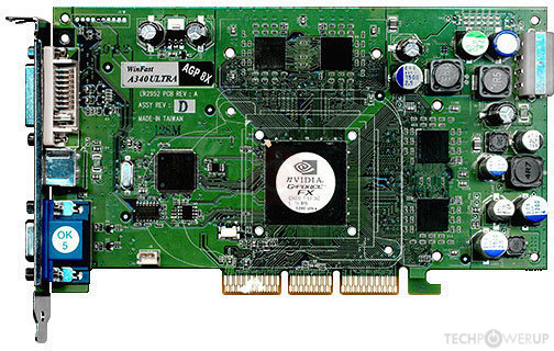
The GeForce FX 5200 Ultra was a mid-range graphics card by NVIDIA, launched on March 6th, 2003. Built on the 150 nm process, and based on the NV34 graphics processor, in its NV34 5200 Ultra variant, the card supports DirectX 9.0a. Since GeForce FX 5200 Ultra does not support DirectX 11 or DirectX 12, it might not be able to run all the latest games. The NV34 graphics processor is an average sized chip with a die area of 124 mm² and 45 million transistors. It features 4 pixel shaders and 2 vertex shaders, 4 texture mapping units, and 4 ROPs. Due to the lack of unified shaders you will not be able to run recent games at all (which require unified shader/DX10+ support). NVIDIA has paired 128 MB DDR memory with the GeForce FX 5200 Ultra, which are connected using a 128-bit memory interface. The GPU is operating at a frequency of 325 MHz, memory is running at 325 MHz.
Being a single-slot card, the NVIDIA GeForce FX 5200 Ultra draws power from 1x Molex power connector, with power draw not exactly known. Display outputs include: 1x DVI, 1x VGA, 1x S-Video. GeForce FX 5200 Ultra is connected to the rest of the system using an AGP 8x interface. The card measures 171 mm in length, and features a single-slot cooling solution. Its price at launch was 149 US Dollars.
Being a single-slot card, the NVIDIA GeForce FX 5200 Ultra draws power from 1x Molex power connector, with power draw not exactly known. Display outputs include: 1x DVI, 1x VGA, 1x S-Video. GeForce FX 5200 Ultra is connected to the rest of the system using an AGP 8x interface. The card measures 171 mm in length, and features a single-slot cooling solution. Its price at launch was 149 US Dollars.
Graphics Processor
Graphics Card
- Release Date
- Mar 6th, 2003
- Generation
-
GeForce FX
(5200)
- Predecessor
- GeForce 4 Ti
- Successor
- GeForce 6 AGP
- Production
- End-of-life
- Launch Price
- 149 USD
- Bus Interface
- AGP 8x
Clock Speeds
- GPU Clock
- 325 MHz
- Memory Clock
-
325 MHz
650 Mbps effective
Memory
- Memory Size
- 128 MB
- Memory Type
- DDR
- Memory Bus
- 128 bit
- Bandwidth
- 10.40 GB/s
Render Config
- Pixel Shaders
- 4
- Vertex Shaders
- 2
- TMUs
- 4
- ROPs
- 4
Theoretical Performance
- Pixel Rate
- 1.300 GPixel/s
- Vertex Rate
- 162.5 MVertices/s
- Texture Rate
- 1.300 GTexel/s
Board Design
- Slot Width
- Single-slot
- Length
- 171 mm
6.7 inches
- TDP
- unknown
- Suggested PSU
- 200 W
- Outputs
- 1x DVI
1x VGA
1x S-Video
- Power Connectors
- 1x Molex
Graphics Features
- DirectX
- 9.0a
- OpenGL
-
1.5 (full)
2.0 (partial)
- OpenCL
- N/A
- Vulkan
- N/A
- Pixel Shader
- 2.0a
- Vertex Shader
- 2.0a
NV34 GPU Notes
| OpenGL 2.0: 60% Support |
May 3rd, 2024 21:39 EDT
change timezone
Latest GPU Drivers
New Forum Posts
- Should I install Windows 10 or 11 for my new device (65)
- NASA Achieves milestone Solid State Battery (215)
- fastest usb cable /transfer (16)
- Only some humans can see refresh rates faster than others, I am one of those humans. (9)
- Need help with a persistent infection possible rootkit or other device. (14)
- TechPowerUp Screenshot Thread (MASSIVE 56K WARNING) (4215)
- Outer Worlds getting boring (37)
- Change GPU or PSU ? Games look cryspy and sharp with microsuttering (1)
- FINAL FANTASY XIV: Dawntrail Official Benchmark (80)
- Announcement: VPN's no longer work right in Windows 10 or 11 or Servers (33)
Popular Reviews
- ASRock NUC BOX-155H (Intel Core Ultra 7 155H) Review
- Meze Audio LIRIC 2nd Generation Closed-Back Headphones Review
- Finalmouse UltralightX Review
- Montech Sky Two GX Review
- Gigabyte GeForce RTX 4070 Ti Super Gaming OC Review
- Upcoming Hardware Launches 2023 (Updated Feb 2024)
- HYTE THICC Q60 240 mm AIO Review
- Alienware Pro Wireless Gaming Keyboard Review
- Ugreen NASync DXP4800 Plus Review
- Team Group T-Force Vulcan ECO DDR5-6000 32 GB CL38 Review
Controversial News Posts
- Intel Statement on Stability Issues: "Motherboard Makers to Blame" (235)
- Windows 11 Now Officially Adware as Microsoft Embeds Ads in the Start Menu (167)
- Sony PlayStation 5 Pro Specifications Confirmed, Console Arrives Before Holidays (117)
- AMD's RDNA 4 GPUs Could Stick with 18 Gbps GDDR6 Memory (114)
- AMD to Redesign Ray Tracing Hardware on RDNA 4 (113)
- NVIDIA Points Intel Raptor Lake CPU Users to Get Help from Intel Amid System Instability Issues (106)
- AMD "Strix Halo" Zen 5 Mobile Processor Pictured: Chiplet-based, Uses 256-bit LPDDR5X (103)
- AMD Ryzen 9 7900X3D Now at a Mouth-watering $329 (103)