AMD "Zen 4" 2021 Launch On Track as TSMC Optimistic About 5 nm
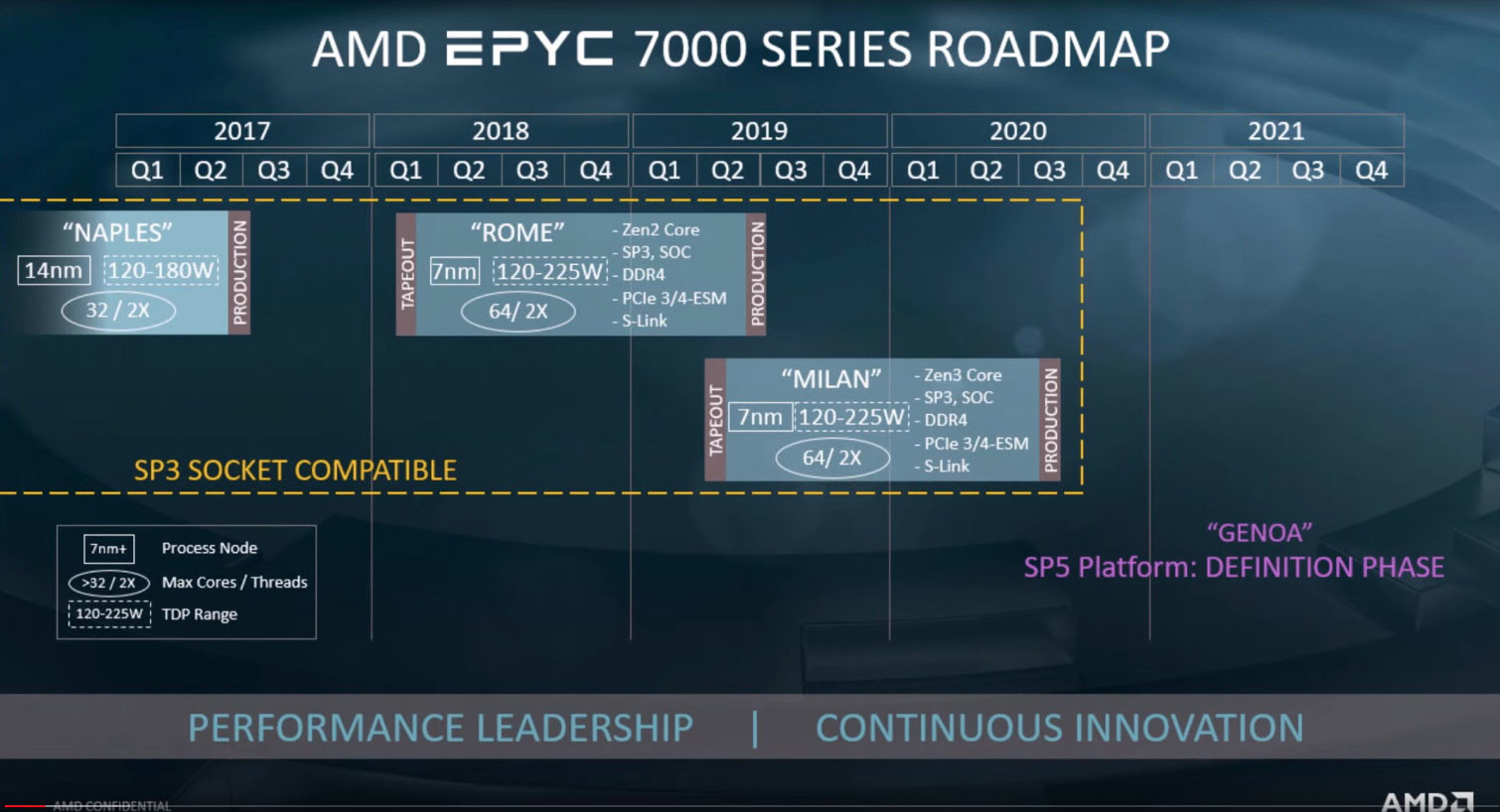
AMD's "Zen 4" CPU microarchitecture is on track for a 2021 launch as its principal foundry partner, TSMC, is optimistic about early yields of its 5 nm silicon fabrication node. TSMC supports the 5 nm product roadmaps of not just AMD, but also Apple and HiSilicon. "Zen 4" is particularly important for AMD, as it will release its next enterprise platform, codenamed "Genoa," along with the new SP5 socket. The new socket will present AMD with the opportunity to significantly change the processor's I/O, such as support for a new memory standard, a new PCIe generation, more memory channels, more PCIe lanes, etc. As early as 2019, the foundry is seeing yields of over 50 percent for the 5 nm node (possibly risk production designed to test the node), which is very encouraging for its customers.
AMD's roadmap for 2020 sees the introduction of "Zen 3" on the 7 nm EUV process (dubbed 7 nm+). AMD recently commented that the performance uplift of "Zen 3" versus "Zen 2" will be "right in line with what you would expect from an entirely new architecture." The 7 nm EUV node provides a significant 20 percent increase in transistor-density compared to the current 7 nm DUV node "Zen 2" chiplets and the company's "Navi" family of GPUs are built on. "Zen 3" could see the company do away with the CCX (quad-core CPU complex), and make chiplets monolithic blocks of CPU cores without sub-divisions. For the client-segment, 5 is a recurring number in 2021. It will see the introduction of the 5th generation Ryzen processors (5000-series), built on the 5 nm process, supporting DDR5 memory, PCI-Express gen 5, and the new AM5 client-segment CPU socket.
AMD's roadmap for 2020 sees the introduction of "Zen 3" on the 7 nm EUV process (dubbed 7 nm+). AMD recently commented that the performance uplift of "Zen 3" versus "Zen 2" will be "right in line with what you would expect from an entirely new architecture." The 7 nm EUV node provides a significant 20 percent increase in transistor-density compared to the current 7 nm DUV node "Zen 2" chiplets and the company's "Navi" family of GPUs are built on. "Zen 3" could see the company do away with the CCX (quad-core CPU complex), and make chiplets monolithic blocks of CPU cores without sub-divisions. For the client-segment, 5 is a recurring number in 2021. It will see the introduction of the 5th generation Ryzen processors (5000-series), built on the 5 nm process, supporting DDR5 memory, PCI-Express gen 5, and the new AM5 client-segment CPU socket.