News Posts matching #HPC

Return to Keyword Browsing

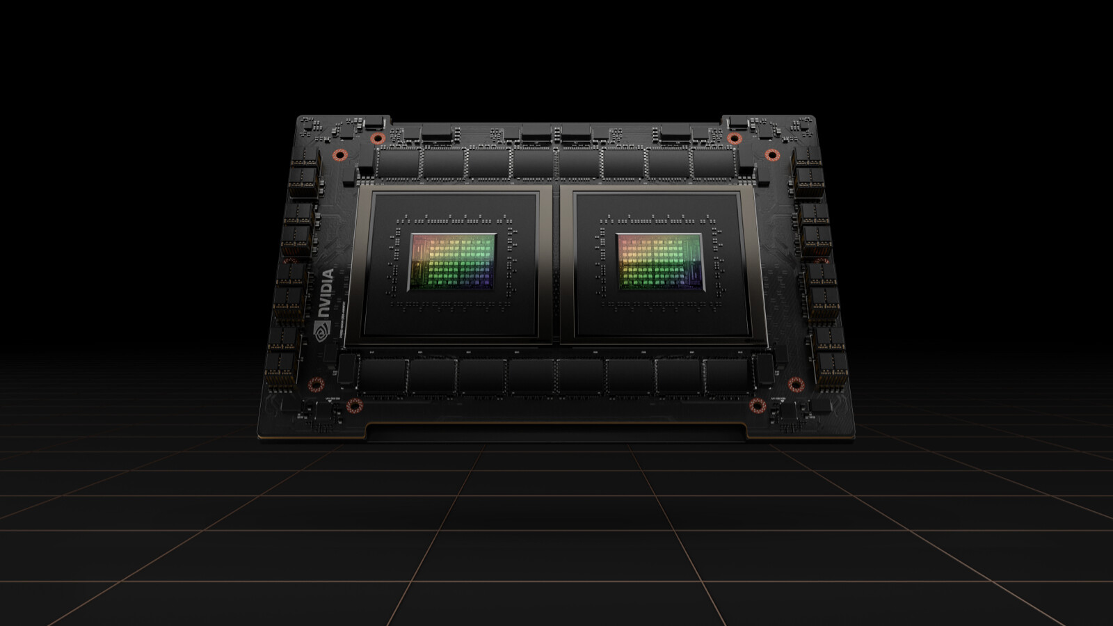
Ayar Labs Partners with NVIDIA to Deliver Light-Based Interconnect for AI Architectures

Ayar Labs, the leader in chip-to-chip optical connectivity, is developing with NVIDIA groundbreaking artificial intelligence (AI) infrastructure based on optical I/O technology to meet future demands of AI and high performance computing (HPC) workloads. The collaboration will focus on integrating Ayar Labs' technology to develop scale-out architectures enabled by high-bandwidth, low-latency and ultra-low-power optical-based interconnects for future NVIDIA products. Together, the companies plan to accelerate the development and adoption of optical I/O technology to support the explosive growth of AI and machine learning (ML) applications and data volumes.

Optical I/O uniquely changes the performance and power trajectories of system designs by enabling compute, memory and networking ASICs to communicate with dramatically increased bandwidth, at lower latency, over longer distances and at a fraction of the power of existing electrical I/O solutions. The technology is also foundational to enabling emerging heterogeneous compute systems, disaggregated/pooled designs, and unified memory architectures that are critical to accelerating future data center innovation.

GIGABYTE Joins Computex to Promote Emerging Enterprise Technologies

GIGABYTE Technology, (TWSE: 2376), an industry leader in high-performance servers and workstations, today announced its participation in Computex, which runs from May 24-27. GIGABYTE's booth will showcase the latest in accelerated computing, liquid & immersion cooling, and edge solutions, as well as provide an opportunity for attendees to get a glimpse at next gen enterprise hardware. GIGABYTE also announced plans to support the NVIDIA Grace CPU Superchip and NVIDIA Grace Hopper Superchip. With the new hardware innovations, GIGABYTE is charting a path to meet the requirements for the foreseeable future in data centers, accordingly many of those important technological modernizations that will be on show at Computex, as well as behind the NDA curtain.

Computex is unquestionably the world's largest computer expo, which has been held annually in Taiwan for over 20 years. Computex has continued to generate great interest and anticipation from the international community. The Nangang Exhibition Center will once again have a strong presence of manufacturers and component buyers encompassing the consumer PC market to enterprise.

HPE Build Supercomputer Factory in Czech Republic

Hewlett Packard Enterprise (NYSE: HPE) today announced its ongoing commitment in Europe by building its first factory in the region for next-generation high performance computing (HPC) and artificial intelligence (AI) systems to accelerate delivery to customers and strengthen the region's supplier ecosystem. The new site will manufacture HPE's industry-leading systems as custom-designed solutions to advance scientific research, mature AL/ML initiatives, and bolster innovation.

The dedicated HPC factory, which will become the fourth of HPE's global HPC sites, will be located in Kutná Hora, Czech Republic, next to HPE's existing European site for manufacturing its industry-standard servers and storage solutions. Operations will begin in summer 2022.

Tachyum Delivers the Highest AI and HPC Performance with the Launch of the World's First Universal Processor

Tachyum today launched the world's first universal processor, Prodigy, which unifies the functionality of a CPU, GPU and TPU in a single processor, creating a homogeneous architecture, while delivering massive performance improvements at a cost many times less than competing products.

After the company undertook its mission to conquer the processor performance plateau in nanometer-class chips and the systems they power, Tachyum has succeeded by launching its first commercial product. The Prodigy Cloud/AI/HPC supercomputer processor chip offers 4x the performance of the fastest Xeon, has 3x more raw performance than NVIDIA's H100 on HPC and has 6x more raw performance on AI training and inference workloads, and up to 10x performance at the same power. Prodigy is poised to overcome the challenges of increasing data center power consumption, low server utilization and stalled performance scaling.

Ayar Labs Raises $130 Million for Light-based Chip-to-Chip Communication

Ayar Labs, the leader in chip-to-chip optical connectivity, today announced that the company has secured $130 million in additional financing led by Boardman Bay Capital Management to drive the commercialization of its breakthrough optical I/O solution. Hewlett Packard Enterprise (HPE) and NVIDIA entered this investment round, joining existing strategic investors Applied Ventures LLC, GlobalFoundries, Intel Capital, and Lockheed Martin Ventures. Other new strategic and financial investors participating in the round include Agave SPV, Atreides Capital, Berkeley Frontier Fund, IAG Capital Partners, Infinitum Capital, Nautilus Venture Partners, and Tyche Partners. They join existing investors such as BlueSky Capital, Founders Fund, Playground Global, and TechU Venture Partners.

"As a successful technology-focused crossover fund operating for over a decade, Ayar Labs represents our largest private investment to date," said Will Graves, Chief Investment Officer at Boardman Bay Capital Management. "We believe that silicon photonics-based optical interconnects in the data center and telecommunications markets represent a massive new opportunity and that Ayar Labs is the leader in this emerging space with proven technology, a fantastic team, and the right ecosystem partners and strategy."

TSMC First Quarter 2022 Financials Show 45.1% Increase in Revenues

A new quarter and another forecast shattering revenue report from TSMC, as the company beat analysts' forecasts by over US$658 million, with a total revenue for the quarter of US$17.6 billion and a net income of almost US$7.26 billion. That's an increase in net income of 45.1 percent or 35.5 percent in sales. Although the monetary figures might be interesting to some, far more interesting details were also shared, such as production updates about future nodes. As a followup on yesterday's news post about 3 nanometer nodes, the N3 node is officially on track for mass production in the second half of this year. TSMC says that customer engagement is stronger than at the start of its N7 and N7 nodes, with HPC and smartphone chip makers lining up to get onboard. The N3E node is, as reported yesterday, expected to enter mass production in the second half of 2023, or a year after N3. Finally, the N2 node is expected in 2025 and won't adhere to TSMC's two year process technology cadence.

Breaking down the revenue by nodes, N7 has taken back the lead over N5, as N7 accounted for 30 percent of TSMC's Q1 revenues up from 27 percent last quarter, but down from 35 percent in the previous year. N5 sits at 20 percent, which is down from 23 percent in the previous quarter, but up from 14 percent a year ago. The 16 and 28 nm nodes still hold on to 25 percent of TSMC's revenue, which is the same as a year ago and up slightly from the previous quarter. Remaining nodes are unchanged from last quarter.

Tachyum Successfully Runs FreeBSD in Prodigy Ecosystem; Expands Open-Source OS Support

Tachyum today announced it has completed validation of its Prodigy Universal Processor and software ecosystem with the operating system FreeBSD, and completed the Prodigy instruction set architecture (ISA) for FreeBSD porting. FreeBSD powers modern servers, desktops, and embedded platforms in environments that value performance, stability, and security. It is the platform of choice for many of the busiest websites and the most pervasive embedded networking and storage devices.

The validation of FreeBSD extends Tachyum's support for open-source operating systems and tools, including Linux, Yocto Project, PHP, MariaDB, PostgreSQL, Apache, QEMU, Git, RabbitMQ, and more.

NVIDIA Claims Grace CPU Superchip is 2X Faster Than Intel Ice Lake

When NVIDIA announced its Grace CPU Superchip, the company officially showed its efforts of creating an HPC-oriented processor to compete with Intel and AMD. The Grace CPU Superchip combines two Grace CPU modules that use the NVLink-C2C technology to deliver 144 Arm v9 cores and 1 TB/s of memory bandwidth. Each core is Arm Neoverse N2 Perseus design, configured to achieve the highest throughput and bandwidth. As far as performance is concerned, the only detail NVIDIA provides on its website is the estimated SPECrate 2017_int_base score of over 740. Thanks to the colleges over at Tom's Hardware, we have another performance figure to look at.

NVIDIA has made a slide about comparison with Intel's Ice Lake server processors. One Grace CPU Superchip was compared to two Xeon Platinum 8360Y Ice Lake CPUs configured in a dual-socket server node. The Grace CPU Superchip outperformed the Ice Lake configuration by two times and provided 2.3 times the efficiency in WRF simulation. This HPC application is CPU-bound, allowing the new Grace CPU to show off. This is all thanks to the Arm v9 Neoverse N2 cores pairing efficiently with outstanding performance. NVIDIA made a graph showcasing all HPC applications running on Arm today, with many more to come, which you can see below. Remember that NVIDIA provides this information, so we have to wait for the 2023 launch to see it in action.

Intel Planning a Return to HEDT with "Alder Lake-X"?

Enthused with its IPC leadership, Intel is possibly planning a return to the high-end desktop (HEDT) market segment, with the "Alder Lake-X" line of processors, according to a Tom's Hardware report citing a curious-looking addition to an AIDA64 beta change-log. The exact nature of "Alder Lake-X" (ADL-X) still remains a mystery—one theory holds that ADL-X could be a consumer variant of the "Sapphire Rapids" microarchitecture, much like how the 10th Gen Core "Cascade Lake-X" was to "Cascade Lake," a server processor microarchitecture. Given that Intel is calling it "Alder Lake-X" and not "Sapphire Rapids-X," it could even be a whole new client-specific silicon. What's the difference between the two? It's all in the cores.

While both "Alder Lake" and "Sapphire Rapids" come with "Golden Cove" performance cores (P-cores), they use variants of it. Alder Lake has the client-specific variant with 1.25 MB L2 cache, a lighter client-relevant ISA, and other optimizations that enable it to run at higher clock speeds. Sapphire Rapids, on the other hand, will use a server-specific variant of "Golden Cove" that's optimized for the Mesh interconnect, has 2 MB of L2 cache, a server/HPC-relevant ISA, and a propensity to run at lower clock speeds, to support the silicon's overall TDP and high CPU core-count.

Fujitsu Achieves Major Technical Milestone with World's Fastest 36 Qubit Quantum Simulator

Fujitsu has successfully developed the world's fastest quantum computer simulator capable of handling 36 qubit quantum circuits on a cluster system featuring Fujitsu's "FUJITSU Supercomputer PRIMEHPC FX 700" ("PRIMEHPC FX 700")(1), which is equipped with the same A64FX CPU that powers the world's fastest supercomputer, Fugaku.

The newly developed quantum simulator can execute the quantum simulator software "Qulacs"(3) in parallel at high speed, achieving approximately double the performance of other significant quantum simulators in 36 qubit quantum operations. Fujitsu's new quantum simulator will serve as an important bridge towards the development of quantum computing applications that are expected to be put to practical use in the years ahead.

TSMC Ramps up Shipments to Record Levels, 5/4 nm Production Lines at Capacity

According to DigiTimes, TSMC is working on increased its monthly shipments of finished wafers from 120,000 to 150,000 for its 5 nm nodes, under which 4 nm also falls. This is three times as much as what TSMC was producing just a year ago. The 4 nm node is said to be in full mass production now and the enhanced N4P node should be ready for mass production in the second half of 2022, alongside N3B. This will be followed by the N4X and N3E nodes in 2023. The N3B node is expected to hit 40-50,000 wafers initially, before ramping up from there, assuming everything is on track.

The report also mentions that TSMC is expecting a 20 percent revenue increase from its 28 to 7 nm nodes this year, which shows that even these older nodes are being heavily utilised by its customers. TSMC has what NVIDIA would call a demand problem, as the company simply can't meet demand at the moment, with customers lining up to be able to get a share of any additional production capacity. NVIDIA is said to have paid TSMC at least US$10 billion in advance to secure manufacturing capacity for its upcoming products, both for consumer and enterprise products. TSMC's top three HPC customers are also said to have pre-booked capacity on the upcoming 3 and 2 nm nodes, so it doesn't look like demand is going to ease up anytime soon.

NVIDIA Unveils Grace CPU Superchip with 144 Cores and 1 TB/s Bandwidth

NVIDIA has today announced its Grace CPU Superchip, a monstrous design focused on heavy HPC and AI processing workloads. Previously, team green has teased an in-house developed CPU that is supposed to go into servers and create an entirely new segment for the company. Today, we got a more detailed look at the plan with the Grace CPU Superchip. The Superchip package represents a package of two Grace processors, each containing 72 cores. These cores are based on Arm v9 in structure set architecture iteration and two CPUs total for 144 cores in the Superchip module. These cores are surrounded by a now unknown amount of LPDDR5x with ECC memory, running at 1 TB/s total bandwidth.

NVIDIA Grace CPU Superchip uses the NVLink-C2C cache coherent interconnect, which delivers 900 GB/s bandwidth, seven times more than the PCIe 5.0 protocol. The company targets two-fold performance per Watt improvement over today's CPUs and wants to bring efficiency and performance together. We have some preliminary benchmark information provided by NVIDIA. In the SPECrate2017_int_base integer benchmark, the Grace CPU Superchip scores over 740 points, which is just the simulation for now. This means that the performance target is not finalized yet, teasing a higher number in the future. The company expects to ship the Grace CPU Superchip in the first half of 2023, with an already supported ecosystem of software, including NVIDIA RTX, HPC, NVIDIA AI, and NVIDIA Omniverse software stacks and platforms.
NVIDIA Grace CPU Superchip

NVIDIA GTC 2022 Keynote Liveblog: NVIDIA Hopper Architecture Unveil

NVIDIA today kicked off the 2022 Graphics Technology Conference, its annual gathering of compute and gaming developers discovering the very next in AI, data-science, HPC, graphics, autonomous machines, edge computing, and networking. At the 2022 show premiering now, NVIDIA is expected to unveil its next-generation "Hopper" architecture, which could make its debut as an AI/HPC product, much like "Ampere." Stay tuned for our live blog!

15:00 UTC: The show gets underway with a thank-you to the sponsors.

AMD Introduces Instinct MI210 Data Center Accelerator for Exascale-class HPC and AI in a PCIe Form-Factor

AMD today announced a new addition to the Instinct MI200 family of accelerators. Officially titled Instinct MI210 accelerator, AMD tries to bring exascale-class technologies to mainstream HPC and AI customers with this model. Based on CDNA2 compute architecture built for heavy HPC and AI workloads, the card features 104 compute units (CUs), totaling 6656 Streaming Processors (SPs). With a peak engine clock of 1700 MHz, the card can output 181 TeraFLOPs of FP16 half-precision peak compute, 22.6 TeraFLOPs peak FP32 single-precision, and 22.6 TFLOPs peak FP62 double-precision compute. For single-precision matrix (FP32) compute, the card can deliver a peak of 45.3 TFLOPs. The INT4/INT8 precision settings provide 181 TOPs, while MI210 can compute the bfloat16 precision format with 181 TeraFLOPs at peak.

The card uses a 4096-bit memory interface connecting 64 GBs of HMB2e to the compute silicon. The total memory bandwidth is 1638.4 GB/s, while memory modules run at a 1.6 GHz frequency. It is important to note that the ECC is supported on the entire chip. AMD provides an Instinct MI210 accelerator as a PCIe solution, based on a PCIe 4.0 standard. The card is rated for a TDP of 300 Watts and is cooled passively. There are three infinity fabric links enabled, and the maximum bandwidth of the infinity fabric link is 100 GB/s. Pricing is unknown; however, availability is March 22nd, which is the immediate launch date.

AMD places this card directly aiming at NVIDIA A100 80 GB accelerator as far as the targeted segment, with emphasis on half-precision and INT4/INT8 heavy applications.

Intel to Invest Over €33 Billion for Semiconductor R&D and Manufacturing in EU

Intel today announced the first phase of its plans to invest as much as 80 billion euros in the European Union over the next decade along the entire semiconductor value chain - from research and development (R&D) to manufacturing to state-of-the art packaging technologies. Today's announcement includes plans to invest an initial 17 billion euros into a leading-edge semiconductor fab mega-site in Germany, to create a new R&D and design hub in France, and to invest in R&D, manufacturing and foundry services in Ireland, Italy, Poland and Spain. With this landmark investment, Intel plans to bring its most advanced technology to Europe, creating a next-generation European chip ecosystem and addressing the need for a more balanced and resilient supply chain.

Pat Gelsinger, CEO of Intel, said: "Our planned investments are a major step both for Intel and for Europe. The EU Chips Act will empower private companies and governments to work together to drastically advance Europe's position in the semiconductor sector. This broad initiative will boost Europe's R&D innovation and bring leading-edge manufacturing to the region for the benefit of our customers and partners around the world. We are committed to playing an essential role in shaping Europe's digital future for decades to come."

Storage Specialist Excelero Joins NVIDIA

Excelero, a Tel Aviv-based provider of high-performance software-defined storage, is now a part of NVIDIA. The company's team of engineers—including its seasoned co-founders with decades of experience in HPC, storage and networking—bring deep expertise in the block storage that large businesses use in storage-area networks.

Now their mission is to help expand support for block storage in our enterprise software stack such as clusters for high performance computing. Block storage also has an important role to play inside the DOCA software framework that runs on our DPUs.

Marvell Introduces Industry's First 800G Multimode Electro-Optics Platform for Cloud Data Centers

Marvell (NASDAQ: MRVL) today announced the industry's first 800 Gbps or 8x 100 Gbps multimode platform solution, that enables data center infrastructure to achieve dramatically higher speeds for short-reach optical modules and Active Optical Cable (AOC) applications. As artificial intelligence (AI), machine learning (ML) and high-performance computing (HPC) applications continue to drive greater bandwidth requirements, cloud-optimized solutions are needed that can bring lower power, latency and cost to short-range data center interconnections. The new 800G platform, which includes Marvell's PAM4 DSP with a multimode transimpedance amplifier (TIA) and Driver, enables faster data center speeds scaling to 800 Gbps, using conventional cost-effective vertical-cavity surface-emitting laser (VCSEL) technology while accelerating time-to-market with plug-and-play deployment.

Today's data centers are packed with equipment utilizing optical modules or AOCs connected by multimode optical fiber optimized for communication over short distances within data centers. This 100G per lane multimode fiber provides cost-effective, low-power, short-reach connectivity. To support multi-gigabit transmissions, multimode architectures often use VCSEL transmitters, which offer the cost benefits of reliability, power efficiency and easy deployment.

GIGABYTE Introduces Direct Liquid Cooled Servers Supercharged by NVIDIA

GIGABYTE Technology, today introduced two new liquid cooled HPC and AI training servers, G262-ZL0 and G492-ZL2, that can push the NVIDIA HGX A100 accelerators and AMD EPYC 7003 processors to the limit with enterprise-grade liquid cooling. To prevent overheating and server downtime in a compute dense data center, GIGABYTE worked with CoolIT Systems to develop a thermal solution that uses direct-liquid cooling to balance optimal performance, high availability, and efficient cooling.

For innovators and researchers in HPC, AI, and data analytics that demand a high level of CPU and GPU compute the new servers are built for the top-tier AMD EPYC 7003 processor and GPU baseboard, NVIDIA HGX A100 80 GB accelerator. Combining components well-designed for performance and efficiency enables much faster insights and results, which users appreciate while reaping the benefits of the value and lower TCO.

Intel Details Ponte Vecchio Accelerator: 63 Tiles, 600 Watt TDP, and Lots of Bandwidth

During the International Solid-State Circuits Conference (ISSCC) 2022, Intel gave us a more significant look at its upcoming Ponte Vecchio HPC accelerator and how it operates. So far, Intel convinced us that the company created Ponte Vecchio out of 47 tiles glued together in one package. However, the ISSCC presentation shows that the accelerator is structured rather interestingly. There are 63 tiles in total, where 16 are reserved for compute, eight are used for RAMBO cache, two are Foveros base tiles, two represent Xe-Link tiles, eight are HBM2E tiles, and EMIB connection takes up 11 tiles. This totals for about 47 tiles. However, an additional 16 thermal tiles used in Ponte Vecchio regulate the massive TDP output of this accelerator.

What is interesting is that Intel gave away details of the RAMBO cache. This novel SRAM technology uses four banks of 3.75 MB groups total of 15 MB per tile. They are connected to the fabric at 1.3 TB/s connection per chip. In contrast, compute tiles are connected at 2.6 TB/s speeds to the chip fabric. With eight RAMBO cache tiles, we get an additional 120 MB SRAM present. The base tile is a 646 mm² die manufactured in Intel 7 semiconductor process and contains 17 layers. It includes a memory controller, the Fully Integrated Voltage Regulators (FIVR), power management, 16-lane PCIe 5.0 connection, and CXL interface. The entire area of Ponte Vecchio is rather impressive, as 47 active tiles take up 2,330 mm², whereas when we include thermal dies, the total area jumps to 3,100 mm². And, of course, the entire package is much larger at 4,844 mm², connected to the system with 4,468 pins.

Intel Updates Technology Roadmap with Data Center Processors and Game Streaming Service

At Intel's 2022 Investor Meeting, Chief Executive Officer Pat Gelsinger and Intel's business leaders outlined key elements of the company's strategy and path for long-term growth. Intel's long-term plans will capitalize on transformative growth during an era of unprecedented demand for semiconductors. Among the presentations, Intel announced product roadmaps across its major business units and key execution milestones, including: Accelerated Computing Systems and Graphics, Intel Foundry Services, Software and Advanced Technology, Network and Edge, Technology Development, More: For more from Intel's Investor Meeting 2022, including the presentations and news, please visit the Intel Newsroom and Intel.com's Investor Meeting site.

Congatec Launches COM-HPC Carrier Design Guide Compliant Ecosystem

congatec welcomes the publication of the COM-HPC Carrier Board Design Guide by the PCI Industrial Computer Manufacturers Group (PICMG) with the launch of a fully specification compliant ecosystem for engineers of COM-HPC Client and Server module based designs. From now on, engineers can dive right in and start to develop fully compliant designs by picking their appropriate Computer-on-Module, add a COM-HPC Server or COM-HPC Client evaluation carrier and appropriate cooling solution, install their application and run programming, debugging and test routines on this new high-performance embedded computing standard.

The congatec COM-HPC ecosystem is fully compliant to the entire range of new PICMG COM-HPC specifications, namely the COM-HPC Module Base Specification, the brand new Carrier Board Design Guide, the Embedded EEPROM specification and the Platform Management Interface specification. Supported by all leading embedded computing vendors, including congatec, this set of PICMG standards offers engineers the benefits of best in class design security.

Google Cloud Chooses 3rd Gen AMD EPYC Processors to Power New Compute Focused Instance

AMD (NASDAQ: AMD) today announced that AMD EPYC processors will power the new C2D virtual machine offering from Google Cloud, bringing customers strong performance and compute power for high-performance (HPC) memory-bound workloads in areas like electronic design automation (EDA) and computational fluid dynamics (CFD). This announcement continues the momentum for AMD EPYC processors, marking the third family of instances powered by 3rd Gen EPYC processors at Google Cloud, joining the T2D and N2D instances.

With the help of AMD EPYC processors and its high core density, the C2D VMs will provide the largest VM sizes within compute optimized family at Google Cloud. As well, because of the EPYC processor's performance for compute focused workloads, Google Cloud showcased the C2D VMs can provide up to 30 percent better performance for targeted workloads compared to previous generation EPYC based VMs at a comparable size.

EuroHPC Joint Undertaking Launches Three New Research and Innovation Projects

The European High Performance Computing Joint Undertaking (EuroHPC JU) has launched 3 new research and innovation projects. The projects aim to bring the EU and its partners in the EuroHPC JU closer to developing independent microprocessor and HPC technology and advance a sovereign European HPC ecosystem. The European Processor Initiative (EPI SGA2), The European PILOT and the European Pilot for Exascale (EUPEX) are interlinked projects and an important milestone towards a more autonomous European supply chain for digital technologies and specifically HPC.

With joint investments of €140 million from the European Union (EU) and the EuroHPC JU Participating States, the three projects will carry out research and innovation activities to contribute to the overarching goal of securing European autonomy and sovereignty in HPC components and technologies, especially in anticipation of the European exascale supercomputers.

Lenovo Unveils TruScale HPC as a Service

Lenovo today unveiled Lenovo TruScale High Performance Computing as a Service (HPCaaS), delivering the power of supercomputing to organizations of all sizes through a cloud-like experience. The new high performance computing (HPC) as-a-service (aaS) offering expands Lenovo's everything as-a-service TruScale portfolio and enables HPC customers to access greater supercomputing resources, driving a faster time to answer for researchers working on solving humanity's greatest challenges.

Cloud-based HPC is the fastest growing segment of high-performance computing, and on-demand resource consumption provides more efficient and scalable computing resources to meet workload requirements. The typical HPC cluster runs at nearly full capacity, with rapidly increasing demands for compute and storage cycles and little room for additional workloads. Lenovo TruScale HPCaaS delivers additional capacity that allows research institutions to better compete for grants while gaining faster insights. The technology provides rack-to-cloud level solutions that are critical to drive innovation across multiple sectors, including academia, pharma, manufacturing and healthcare.

JEDEC Publishes HBM3 Update to High Bandwidth Memory (HBM) Standard

JEDEC Solid State Technology Association, the global leader in the development of standards for the microelectronics industry, today announced the publication of the next version of its High Bandwidth Memory (HBM) DRAM standard: JESD238 HBM3, available for download from the JEDEC website. HBM3 is an innovative approach to raising the data processing rate used in applications where higher bandwidth, lower power consumption and capacity per area are essential to a solution's market success, including graphics processing and high-performance computing and servers.
Return to Keyword Browsing
May 7th, 2024 22:29 EDT change timezone

New Forum Posts

Popular Reviews

Controversial News Posts