News Posts matching #Hawaii

Return to Keyword Browsing

AMD "Navi" Features 8 Streaming Engines, Possible ROP Count Doubling?

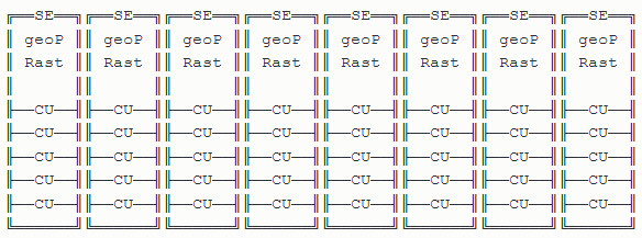
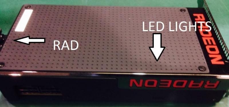
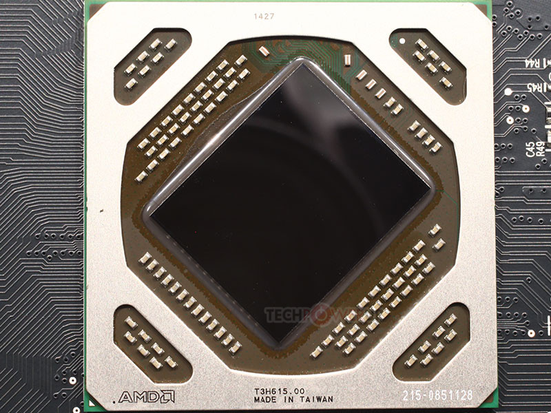
AMD's 7 nm "Navi 10" silicon may finally address two architectural shortcomings of its performance-segment GPUs, memory bandwidth, and render-backends (deficiency thereof). The GPU almost certainly features a 256-bit GDDR6 memory interface, bringing about a 50-75 percent increase in memory bandwidth over "Polaris 30." According to a sketch of the GPU's SIMD schematic put out by KOMACHI Ensaka, Navi's main number crunching machinery is spread across eight shader engines, each with five compute units (CUs).

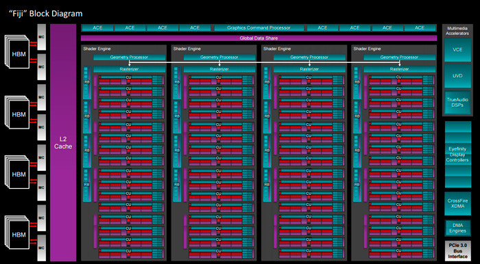
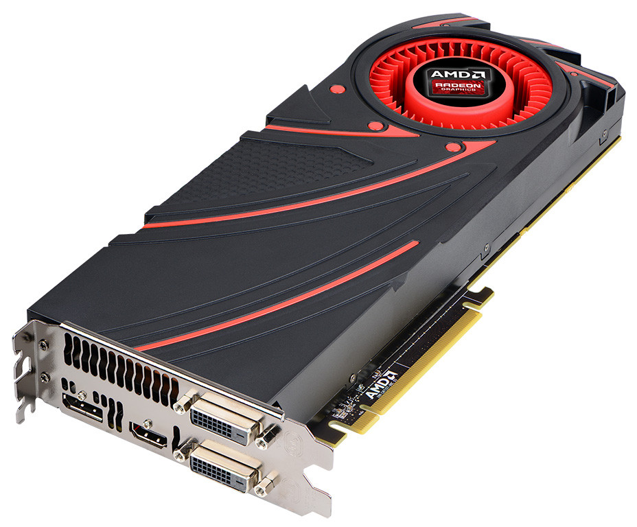
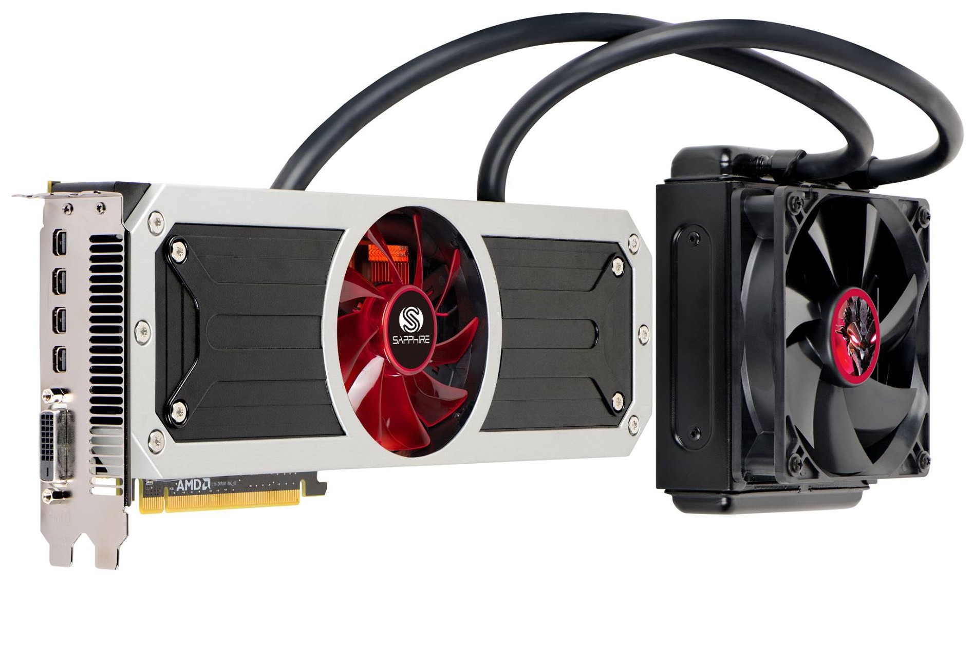
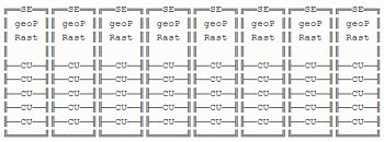
Five CUs spread across eight shader engines, assuming each CU continues to pack 64 stream processors, works out to 2,560 stream processors on the silicon. This arrangement is in stark contrast to the "Hawaii" silicon from 2013, which crammed 10 CUs per shader engine across four shader engines to achieve the same 2,560 SP count on the Radeon R9 290. The "Fiji" silicon that followed "Hawaii" stuck to the 4-shader engine arrangement. Interestingly, both these chips featured four render-backends per shader engine, working out to 64 ROPs. AMD's decision to go with 8 shader engines raises hopes for the company doubling ROP counts over "Polaris," to 64, by packing two render backends per shader engine. AMD unveils Navi in its May 27 Computex keynote, followed by a possible early-July launch.

AMD "Vega" Die-shot Revealed

AMD released the die-shot of its "Vega 10" ASIC. The multi-chip module (MCM) of the GPU die and two HBM2 memory stacks, sitting on a silicon interposer, is slightly smaller than the "Fiji" ASIC, as it features just two memory stacks. AMD didn't label the components of the GPU die, but we can make out 8 shader engines, holding 8 GCN compute units (CUs), each. This is unlike "Fiji," where the GPU holds four engines with 16 CUs, each. This would mean that each group of 8 CUs has its own dedicated geometry processor and rasterizer.

Since each CU holds 64 FP32 stream processors, we arrive at the total stream processor count of 4,096. Unlike "Hawaii," these stream-processors are FP16-capable, so simple compute tasks are handled at double the throughput. We also make out 32 render back-ends, double that of "Fiji" and "Hawaii," which could indicate 128 ROPs. The "Vega 10" ASIC features a 2048-bit HBM2 memory interface.

Update: AMD stated that the die-shot appeared in one of its marketing slides, but may not be real.

AMD "Fiji" Block Diagram Revealed, Runs Cool and Quiet

AMD's upcoming flagship GPU silicon, codenamed "Fiji," which is breaking ground on new technologies, such as HBM, memory-on-package, a specialized substrate layer that connects the GPU with it, called Interposer; features a hefty feature-set. More on the "Fiji" package and its memory implementation, in our older article. Its block diagram (manufacturer-drawn graphic showing the GPU's component hierarchy), reveals a scaling up, of the company's high-end GPU launches over the past few years.

"Fiji" retains the quad Shader Engine layout of "Hawaii," but packs 16 GCN Compute Units (CUs), per Shader Engine (compared to 11 CUs per engine on Hawaii). This works out to a stream processor count of 4,096. Fiji is expected to feature a newer version of the Graphics CoreNext architecture than "Hawaii." The TMU count is proportionately increased, to 256 (compared to 176 on "Hawaii"). AMD doesn't appear to have increased the ROP count, which is still at 64. The most significant change, however, is its 4096-bit HBM memory interface, compared to 512-bit GDDR5 on "Hawaii."

AMD Dual-GPU "Fiji" Graphics Card PCB Pictured

Here is the first reasonably detailed PCB shot of the dual-GPU graphics card based on "Fiji," which AMD announced at its E3 conference. The card is an inch taller than standard, but surprisingly short, for a dual-GPU board. This is thanks to the memory being relocated to the GPU package. All that's left on the PCB, besides the two GPUs, are the PLX PEX8747 PCI-Express gen 3.0 x48 bridge chip, and the 12-phase VRM, which draws power from a pair of 8-pin PCIe power connectors. Display outputs include one HDMI 2.0, and three DisplayPort 1.2a connectors.

AMD announced significant energy efficiency gains for "Fiji" over "Hawaii," and so this card could have a much lower than expected power-draw. The reference board could come with AIO liquid-cooling, much like the single-GPU Radeon R9 Fury X, some AIBs could even release cards with air-cooling solutions. The yet unnamed dual-GPU "Fiji" based graphics card could be available in Autumn 2015.
Image Credit: Anshel Sag (Twitter)

Radeon R9 390X and R9 390 to Feature Faster Memory, Core Over Predecessors

AMD's upcoming Radeon R9 390X and R9 390 performance-segment graphics cards reportedly feature higher GPU and memory clocks over the products they are a re-branding of, the R9 290X and R9 290, respectively. The 28 nm "Grenada" silicon they are based on, is identical to "Hawaii," down to the last transistor. This has been confirmed by leaked GPU-Z screenshots, which reveal the device-IDs of the two cards to be identical to those of the R9 290X and R9 290. Since the Device-IDs are the same, GPU-Z is reading the chip as "Hawaii." The code-name "Grenada" appears in the BIOS version string.

Unlike older, more blatant re-brands, such as GeForce 8800 GT to 9800 GT, AMD did drop in a few changes. To begin with, the memory amount has been doubled on both cards, to 8 GB. The memory clock has been increased from 1250 MHz (5.00 GHz GDDR5-effective), to 1500 MHz (6.00 GDDR5-effective), resulting in memory bandwidth increase to 384 GB/s, up from 320 GB/s. The core clock speed on the R9 390X is 1050 MHz (up from 1000 MHz on R9 290X); and 1000 MHz on the R9 390 (up from 947 MHz on the R9 290).

Radeon R9 390X Taken Apart, PCB Reveals a Complete Re-brand

People with access to an XFX Radeon R9 390X graphics card, took it apart to take a peek at its PCB. What they uncovered comes as no surprise - the underlying PCB is identical in design to AMD reference PCB for the Radeon R9 290X, down the location of every tiny SMT component. At best, the brands on the chokes and bigger conductive polymer caps differ; and 512 Gbit GDDR5 chips under the heatspreader, making up 8 GB of the standard memory amount. The GPU itself, codenamed "Grenada," looks identical to the "Hawaii" silicon which drove the R9 290 series. It's highly unlikely that it features updated Graphics CoreNext 1.2 stream processors, as older rumors suggested.

AMD Fiji XT Pictured Some More

In the latest picture leaked of AMD's upcoming flagship graphics card, codenamed "Fiji-XT," we get a final confirmation of the reference-design card's length, particularly its short PCB. Since this card uses a factory-fitted AIO liquid cooling solution, and since the Fiji XT package is effectively smaller than that of Hawaii, with the surrounding memory chips gone (moved to the GPU package as HBM stacks), the PCB is extremely compact, with just the GPU package, and its VRM. Speaking of which, the card draws power from a pair of 8-pin PCIe power connectors. The coolant tubes stick out from the rear of the card, making their way to a 120 x 120 mm radiator, with a single included 120 mm PWM fan. With this card, AMD is doing away with DVI altogether. Connectors will be a mixture of DisplayPort 1.2a and HDMI 2.0.

AMD "Fiji" HBM Implementation Detailed

Back in 2008, when it looked like NVIDIA owned the GPU market, and AMD seemed lagging behind on the performance and efficiency game, the company sprung a surprise. The company's RV770 silicon, the first GPU to implement GDDR5 memory, trounced NVIDIA's big and inefficient GeForce GTX 200 series, and threw AMD back in the game. GDDR5 helped the company double the memory bandwidth, with lower pin- and memory-chip counts, letting the company and its partners build graphics cards with fewer components, and earn great margins, which the company invested in development of its even better HD 5000 series, that pushed NVIDIA with its comical GeForce GTX 480, to hit its lowest ever in market-share. Could AMD be looking at a similar turnaround this summer?

Since the introduction of its Graphics CoreNext architecture in 2012, AMD has been rather laxed in its product development cycle. The company has come out with a new high-end silicon every 18-24 months, and adopted a strategy of cascading re-branding. The introduction of each new high-end silicon would relegate the existing high-end silicon to the performance segment re-branded, and the existing performance-segment silicon to mid-range, re-branded. While the company could lay out its upcoming Radeon R9 series much in the same way, with the introduction of essentially just one new silicon, "Fiji," it could just prove enough for the company. Much like RV770, "Fiji" is about to bring something that could prove to be a very big feature to the consumer graphics market, stacked high-bandwidth memory (HBM).

AMD Fiji XT Reference PCB as Short as GTX 970 Reference, R9 295X2 Performance

AMD's upcoming Radeon R9 390X graphics cards will ship in two SKUs - an air-cooled one, with a moderately long reference design board (though not as long as the R9 290X), and a new Water-Cooled Edition (WCE) SKU, which will feature a very compact PCB - one that could be no bigger than that of the GeForce GTX 970 reference. This is possible because of AMD's HBM implementation. The 8 GB of memory on this card is present on the GPU package, as bare 3D-stacked DRAM dies, surrounding the GPU die, with an IHS covering everything; rather than the GPU package being surrounded by memory chips. Below is a mock-up of the card by ChipHell. It's not a picture. The radiator is off-proportions, the Radeon logo is misaligned, and the PCIe I/O is misaligned, etc. It should still give you a good idea of what the card looks like, particularly its length. Other specs on hand so far, include 4,096 GCN 1.2 stream processors, 256 TMUs, 128 ROPs, and a 4096-bit wide HBM interface, which at 1.25 GHz memory clock, will offer memory bandwidth of 640 GB/s.

While Fiji package will be bigger than that of, say, "Hawaii," overall the setup is more space-efficient, and conserves PCB real-estate. The PCB hence only has the GPU package and the VRM. AMD is doing away with the DVI connector on its reference PCB. It will only feature three DisplayPort 1.2a and one HDMI 2.0a. The WCE variant will feature a pump+block covering the GPU package, which will come factory-fitted to a 120 x 120 mm radiator. The air-cooled R9 390X will be longer, but only to house a heatsink and lateral blower. The single-GPU card could offer performance comparable to the dual-GPU R9 295X2, which is faster than the GeForce GTX TITAN-X. AMD CEO Lisa Su, speaking at the Investor Day event, in New York, on 6th May, hinted that the product could launch on the sidelines of either Computex 2015 (early-June) or E3 (mid-June).
Image Courtesy: ChipHell. Many Thanks to GhostRyder for the tip.

AMD Radeon R9 380 Launched by PC OEM

Earlier this day, HP announced its newest line of desktop PCs, one of which comes with a curious-sounding Radeon R9 380 graphics card. HP's product pages for its new desktops aren't active, yet, leaving us to only speculate on what the R9 380 could be. One theory making rounds says that the R9 380 could either be a re-branded R9 285, or be based on its "Tonga" silicon, which physically features 2,048 stream processors based on Graphics CoreNext (GCN) 1.2 architecture, and a 384-bit wide GDDR5 memory interface. Another theory states that the R9 380 could be an OEM-only re-brand of the R9 280 or R9 280X, based on the 3+ year old "Tahiti" silicon.

The former theory sounds more plausible, because re-branding a "Tahiti" based product would be suicidal for AMD. Although based on GCN, "Tahiti" lacks a lot of architecture features introduced with "Hawaii" and "Tonga." AMD practically stopped optimizing games for "Tahiti," and some of its new features, such as FreeSync and XDMA CrossFire, can't be implemented on it. "Tonga," on the other hand, supports both these features, and one can create an SKU with all its 2,048 stream processors, and its full 384-bit GDDR5 memory interface unlocked. If the R9 380 is indeed an OEM-only product, then it's likely that the company's retail-channel products could be branded in the succeeding R9 400 series. GPU makers tend to re-brand and bump their SKUs by a series for OEMs to peddle in their "new" products at short notice.

Radeon R9 380X Based on "Grenada," a Refined "Hawaii"

AMD's upcoming Radeon R9 380X and R9 380 graphics cards, with which it wants to immediately address the GTX 980 and GTX 970, will be based on a "new" silicon codenamed "Grenada." Built on the 28 nm silicon fab process, Grenada will be a refined variant of "Hawaii," much in the same way as "Curacao" was of "Pitcairn," in the previous generation.

The Grenada silicon will have the same specs as Hawaii - 2,816 GCN stream processors, 176 TMUs, 64 ROPs, and a 512-bit wide GDDR5 memory interface, holding 4 GB memory. Refinements in the silicon over Hawaii could allow AMD to increase clock speeds, to outperform the GTX 980 and GTX 970. We don't expect the chip to be any more energy efficient at its final clocks, than Hawaii. AMD's design focus appears to be performance. AMD could save itself the embarrassment of a loud reference design cooler, by throwing the chip up for quiet custom-design cooling solutions from AIB (add-in board) partners from day-one.

MSI Announces Radeon R9 290X Gaming 8GB Graphics Card

MSI is proud to announce the availability of the new R9 290X GAMING 8G graphics card. Packed with 8 Gigabyte GDDR5 memory operating at 5500MHz and all the extra features stuffed with it, the new 290X GAMING 8G is sure to drive UltraHD gaming resolutions without any problem. The MSI Twin Frozr IV Advanced ensures your card runs cool so you can enjoy maximum performance while AMD's PowerTune technology enables the R9 290X GAMING 8G to run at highest clock speeds.

With support for the latest industry standards and thrilling new technology such as Mantle support in Battlefield 4. Thanks to the bundled MSI GAMING App gamers can quickly switch between three pre-sets including a silent mode optimized for power efficiency and an overclocking and OC Mode to get the most power out of your graphics card, without worrying about learning how to overclock. The R9 290X GAMING 8G has been designed to give you a fluid and silent gaming experience that delivers you true next-gen performance for 4K UHD resolutions and up, without sacrificing on thermals or noise.

AMD Radeon R9 295X2 to Get Promotional Price, Open to All

AMD announced a series of retailer-specific promotions for its flagship Radeon R9 295X2 dual-GPU graphics card. The card, which launched at US $1,499, will be available for as low as $999, as part of retailer promotions. End users (you), and not just OEMs, will be able to buy the card at the three-figure price. The card will ship with its usual Radeon Rewards package, giving you access to over a dozen free games. Based on a pair of 28 nm "Hawaii" GPUs, the Radeon R9 295X2 features a total of 5,760 Graphics CoreNext 1.1 stream processors, 352 TMUs, and 128 ROPs, split between its two GPUs, and 8 GB of memory across its two 512-bit wide GDDR5 memory interfaces.

NVIDIA to Launch GeForce GTX 880 in September

NVIDIA is expected to unveil its next generation high-end graphics card, the GeForce GTX 880, in September 2014. The company could tease its upcoming products at Gamescom. The company is reportedly holding a huge media event in California this September, where it's widely expected to discuss high-end graphics cards based on the "Maxwell" architecture. Much like AMD's Hawaii press event that predated actual launch of its R9 290 series by several weeks; NVIDIA's event is expected to be a paper-launch of one or more graphics cards based on its GM204 silicon, with market availability expected in time for Holiday 2014 sales.

The GM204 is expected to be NVIDIA's next workhorse chip, which will be marketed as high-end in the GeForce GTX 800 series, and performance-segment in its following GTX 900 series; much like how the company milked its "Kepler" based GK104 across two series. It's expected to be built on the existing 28 nm process, although one cannot rule out an optical shrink to 20 nm later (like NVIDIA shrunk the G92 from 65 nm to 55 nm). The GTX 880 reportedly features around 3,200 CUDA cores, and 4 GB of GDDR5 memory.

AMD FirePro W8100 Pictured

At a conference in early June, AMD accidentally disclosed its upcoming FirePro W8100 professional graphics card, ahead of its launch. A cut-down of the FirePro W9100, the W8100 is based on the 28 nm "Hawaii" silicon, that's binned for higher durability. It features 2,560 GCN2 stream processors, 160 TMUs, 64 ROPs, and a 512-bit wide GDDR5 memory interface, holding 8 GB of memory. Compare those to the 2,816 SPs and 16 GB memory of the W9100. The core on the W8100 is clocked at 825 MHz, at which, it puts out single-precision floating point performance of 4.2 TFLOP/s. The dual-slot card is built on a red PCB that's unlike anything AMD built Radeon brand cards out of. It draws power from two 6-pin PCIe power connectors, is shorter in length than the consumer R9 290 reference board, and features a back-plate, to cool memory chips on the reverse side of the PCB. The card supports DirectX 11.2, OpenGL 4.4, and Mantle. It will likely be positioned against NVIDIA's Quadro K5000, at the US $2,500 range. It will also be one of the GPU options in Dell's Precision T7800 workstations.

AMD Readies 28 nm "Tonga" to Take on GM107

NVIDIA's energy-efficiency leap achieved on existing 28 nanometer process, using the "Maxwell" based GM107, appears to have rattled AMD. The company is reportedly attempting a super-efficient, 28 nm, mid-range chip of its own, codenamed "Tonga." The chip could power graphics cards that compete with the GeForce GTX 750 Ti and GTX 750. The chip is likely to be based on Graphics CoreNext 2.0 micro-architecture, the same one that drives "Hawaii," which means AMD isn't counting on the micro-architecture for efficiency gains. It could feature an evolution of PowerTune, which works closer to the metal than its existing implementation on "Hawaii." Other features could include Mantle, TrueAudio, and perhaps even XDMA CrossFire (no cables needed). The chip could be wired to up to 2 GB of memory.

Another equally plausible theory doing rounds is that "Tonga" could be a replacement to "Tahiti Pro," designed to compete with the GK104 at much lower power footprint (than "Tahiti"), so AMD could more effectively compete with the GeForce GTX 760. The chip could be similar in feature-set to "Tahiti," with a narrower memory bus (256-bit wide), but higher clock speeds to make up for it. If this theory holds true, then "Tonga" could disrupt both Tahiti Pro and "Curacao XT." Curacao XT (R9 270X) is designed to offer a value-conscious alternative to the $250 GTX 760. The R9 280 is competitive in performance, but takes a beating on the energy-efficiency front, and is also costlier to manufacture, due to the higher transistor count and four additional memory chips. We could hear more at Computex 2014.

AMD to Launch New Single-GPU Card This Summer, to Take on GTX 780 Ti

AMD is reportedly working on a new single-GPU graphics card SKU to compete with the likes of GeForce GTX 780 Ti, and perhaps even take a swing at the GTX TITAN Black, since it's not too far ahead of the GTX 780 Ti at single-display gaming. The new SKU will be more than just a clock-speed bump, it will leverage HBM (high-bandwidth memory), a cutting-edge new technology that relies on stacking multiple DRAM dies with dedicated memory paths into a single package, cutting down on power-draw, thermals, and PCB real-estate.

The first kind of HBMs to hit the market are 8 Gbit 4Hi, which will interface with the GPU over a 128-bit wide path, which means there will be just four memory packages on the card (since the "Hawaii" silicon features a 512-bit wide memory bus), with improvements in the area of power-draw and heat output. The memory could be clocked higher, too. Sadly, memory bandwidth is not the prime-mover in VGA performance, and AMD will have to offer higher GPU clocks for the card to stand a chance against NVIDIA's high-end single-GPU offerings. As for the name this card would bear, we get a sense of deja vu about how NVIDIA launched the single-GPU GeForce 7950 GTX alongside the dual-GPU 7950 GX2, replacing the 7900 GTX. And so, it wouldn't surprise us if AMD named it Radeon R9 295X.

Aqua Computer Announces Radeon R9 295X2 Full Cover Block

The German-based liquid cooling specialist Aqua Computer has added the full cover water block kryographics Vesuvius for R9 295X2 cards to its portfolio. The block is entirely made in Germany and milled from 2.72kg high-purity electrolytic copper raw material. It covers the GPUs, all RAM chips, the voltage regulators and the PCIe bridge chip. All areas are covered by the flow path of the cooling liquid to provide an excellent cooling performance.

Both GPUs are covered by a micro structure with a 0.5 mm grid. The water flows through both structures in parallel which allows an even temperature for both GPUs. To achieve this effect the cooling structures use a different depth which makes sure that the same amount of water flows through both of them.

Radeon R9 295X2 Starts Selling

The flagship graphics card from AMD, Radeon R9 295X2, started selling, and is listed by leading retailers worldwide. AMD set the MSRP of this card at US $1,499, the pre-tax price could swing by ±5%. At that price, the R9 295X2 is the costliest reference-design graphics card by AMD, and is currently the fastest one money can buy. A dual-GPU on a stick solution with two 28 nm "Hawaii" GPUs, the R9 295X2 features a total of 5,632 GCN2 stream processors (2,816 per GPU), 352 TMUs (176 per GPU), 128 ROPs (64 per GPU), and a total of 8 GB of memory, across two 512-bit wide memory interfaces. The card is cooled by a factory-fitted water-cooling solution by Asetek.

ASUS Announces its Radeon R9 295X2 Graphics Card

ASUS joined the Radeon R9 295X2 launch party with a card of its own. Sticking to AMD's reference board design, ASUS' offering ships in a big black+red box. The card features reference clock speeds of 1018 MHz core, with 5.00 GHz memory; and 8 GB of memory (2x 4 GB). Its two "Hawaii" GPUs feature 2,816 stream processors, 176 TMUs, 64 ROPs, and 512-bit wide memory interfaces, each. ASUS is pricing the card on par with the others, at US $1,499.

ASUS Radeon R9 295X2 Graphics Card Pictured, Pricing Revealed

Here's the first picture of an AMD add-in board (AIB) branded Radeon R9 295X2 dual-GPU graphics card, ASUS in this case. The card ships in a huge cubical box, although we're not sure if that paperboard box hides a metal suitcase inside. ASUS did away with the perforated metal grille over the central fan on the card, and plastered a couple of stickers, although the rest of the card sticks to AMD's reference board design. According to leading Turkish tech publication DonanimHaber, AMD is planning to price the Radeon R9 295X2 at US $1,499. According to older reports, the R9 295X2 is a dual-GPU CrossFire-on-a-stick graphics card, featuring two 28 nm "Hawaii" GPUs, with all 2,816 stream processors, 176 TMUs, 64 ROPs, and 512-bit wide memory interfaces enabled on each chip, and 4 GB of memory per GPU system, totaling the amount to 8 GB.

Radeon R9 295X2 Press Deck Leaked

Here are some of the key slides from AMD's press-deck (presentation) for reviewers, for the Radeon R9 295X2 dual-GPU graphics card, ahead of its April 8 launch. The slides confirm specifications that surfaced earlier this week, which describe the card as bearing the codename "Vesuvius," having two 28 nm "Hawaii" GPUs, and all 2,816 stream processors on the chips being enabled, next to 176 TMUs, 64 ROPs, and 512-bit wide GDDR5 memory interfaces. Two such chips are wired to a PLX PEX8747 PCI-Express 3.0 x48 bridge chip. There's a total of 8 GB of memory on board, 4 GB per GPU. Lastly, clock speeds are revealed. The GPUs are clocked as high as 1018 MHz, and memory at 5.00 GHz (GDDR5-effective). The total memory bandwidth of the card is hence 640 GB/s.

The Radeon R9 295X2 indeed looks like the card which was pictured earlier this week, by members of the ChipHell tech community. It features an air+liquid hybrid cooling solution, much like the ROG ARES II by ASUS. The cooling solution is co-developed by AMD and Asetek. It features a couple of pump-blocks cooling the GPUs, which are plumbed with a common coolant channel running through a single 120 mm radiator+reservoir unit. A 120 mm fan is included. A centrally located fan on the card ventilates heatsinks that cool the VRM, memory, and the PCIe bridge chip.

Radeon R9 295X2 Pictured in the Flesh, Specs Leaked

Here it is, folks! The first pictures of what you get inside the steel briefcase AMD ships the Radeon R9 295X2 in. AMD got over the stonewall of having to cool two 250W GPUs with a single two-slot cooling solution, by making it an air+liquid hybrid. The cooler appears to have been designed by any of the major water-cooling OEMs (such as Asetek, Akasa, etc.), and most likely consists of a pair of pump-blocks plumbed to a single 120 x 120 mm radiator, over a single coolant loop. The coolant channel, we imagine, could be identical to that of the ROG ARES 2 by ASUS. There's also a 90 mm fan, but that probably cools heatsinks covering the memory, VRM, and PCIe bridge. The card draws power from two 8-pin PCIe power connectors, which as you'll soon find out, are running at off-specs.

The Radeon R9 295X2, codenamed "Vesuvius," runs a pair of 28 nm "Hawaii" chips, routed to a PLX PEX8747 PCIe bridge. Each of the two have all 2,816 stream processors enabled, totaling the count to 5,632. The two also have 352 TMUs, and 128 ROPs between them. The entire 512-bit memory bus width is enabled, and each GPU is wired to 4 GB of memory totaling 8 GB on the card. Clock speeds remain a mystery, and probably hold the key to a lot of things, such as power draw and cooling. Lastly, there's the price. AMD could price the R9 295X2 at US $1,499, half that of NVIDIA's GeForce GTX TITAN-Z. In that price difference, heck, even for $500, you could probably buy yourself a full-coverage water block, and a full-fledged loop, complete with a meaty 3 x 120 mm radiator.

More Details of Radeon R9 295X2 Emerge

More details of AMD's upcoming dual-GPU graphics cards based on the "Hawaii" silicon emerged, in the run up to its April 8 launch. That's right, AMD plans to launch the card exactly one week from now. The card will bear the name Radeon R9 295X2, after all. The $3,000 pricing set by NVIDIA for its GTX TITAN-Z graphics card will be taken advantage of AMD, which will splurge on stuff such as a metal briefcase to ship the card in (with two combi-locks no less!), possibly high-quality (expensive) cooler shroud materials, and more. The card will be cooled by an air+liquid hybrid cooling solution, much like the ASUS ROG ARES 2. A factory-fitted (AIO) liquid cooling loop will handle the two 250W GPUs, while a fan-heatsink will cool the memory, VRM, and PCIe bridge chip. AMD will not chase down the ludicrous 12 GB memory amount of GTX TITAN-Z despite its wider memory bus, and will instead equip it with 8 GB (4 GB per GPU). And lastly, the card will have a total of five display outputs, including four mini-DP and one dual-link DVI-D (digital-only).

AMD "Hawaii" Based Dual GPU Graphics Card Could be Named R9 295X2

AMD's dual-GPU flagship graphics card that runs a pair of 28 nm "Hawaii" GPUs is no unicorn, as the company began teasing the press about it. Dutch tech publication BouweenPC.nl dug up info that points to AMD naming the card "Radeon R9 295X2." The two "Hawaii" GPUs are expected to feature a core clock speed of no less than 1000 MHz, according to the report. It also adds that AMD is working on a air+liquid (hybrid) cooling solution for the card. Its cooler will feature heatsinks with a running air flow to cool the memory, VRM, and other hot ancillary components; while two liquid cooling blocks will dissipate heat form the GPUs. This would also mean that installing the R9 295X2 won't be as simple as pushing it into a PCIe slot, fastening a couple of screws, and plugging the PSU in. ASUS attempted a similar cooling solution for its Republic of Gamers ARES II graphics card.
Return to Keyword Browsing
May 9th, 2024 10:06 EDT change timezone

New Forum Posts

Popular Reviews

Controversial News Posts