News Posts matching #Zen 5

Return to Keyword Browsing

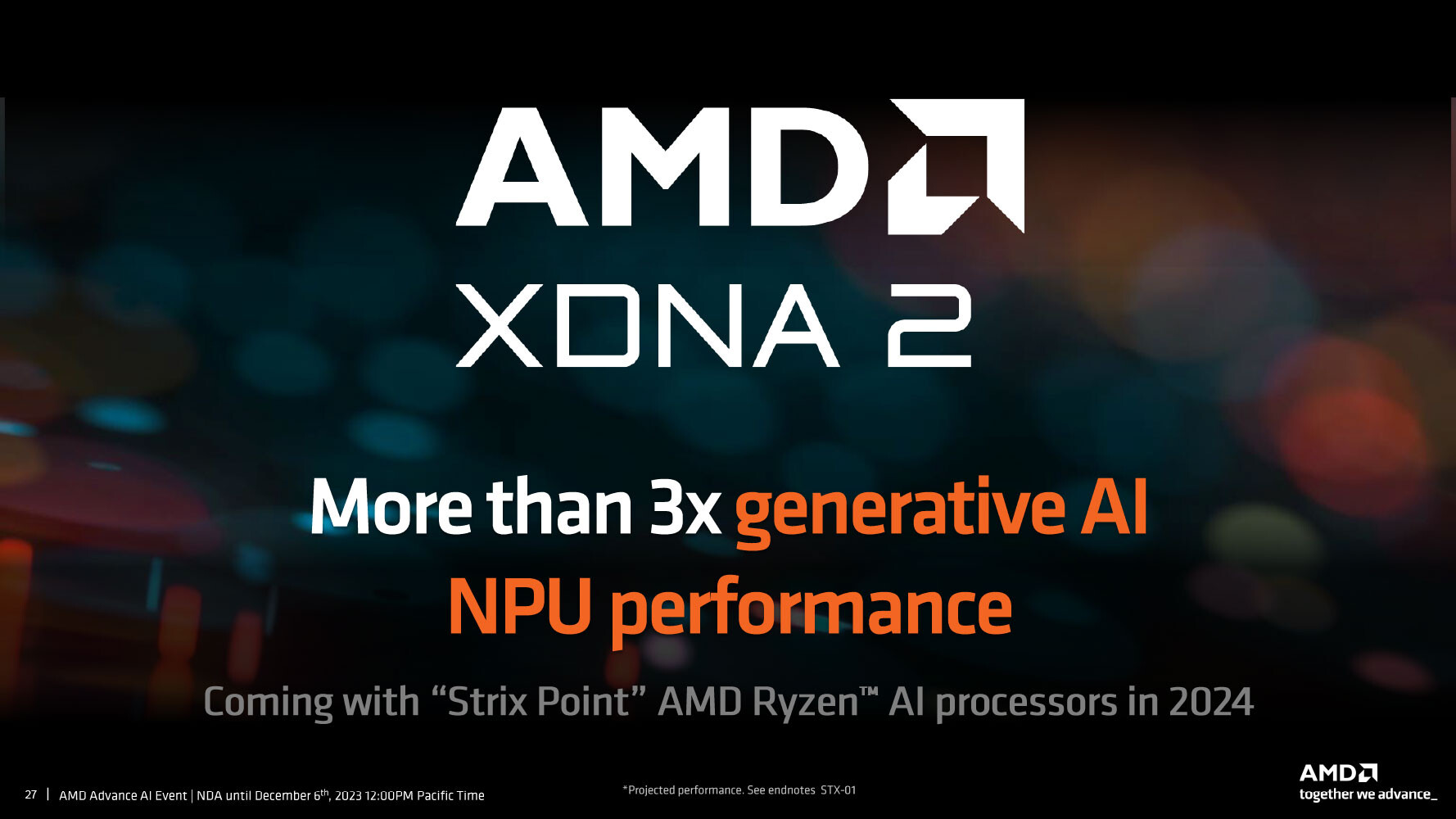
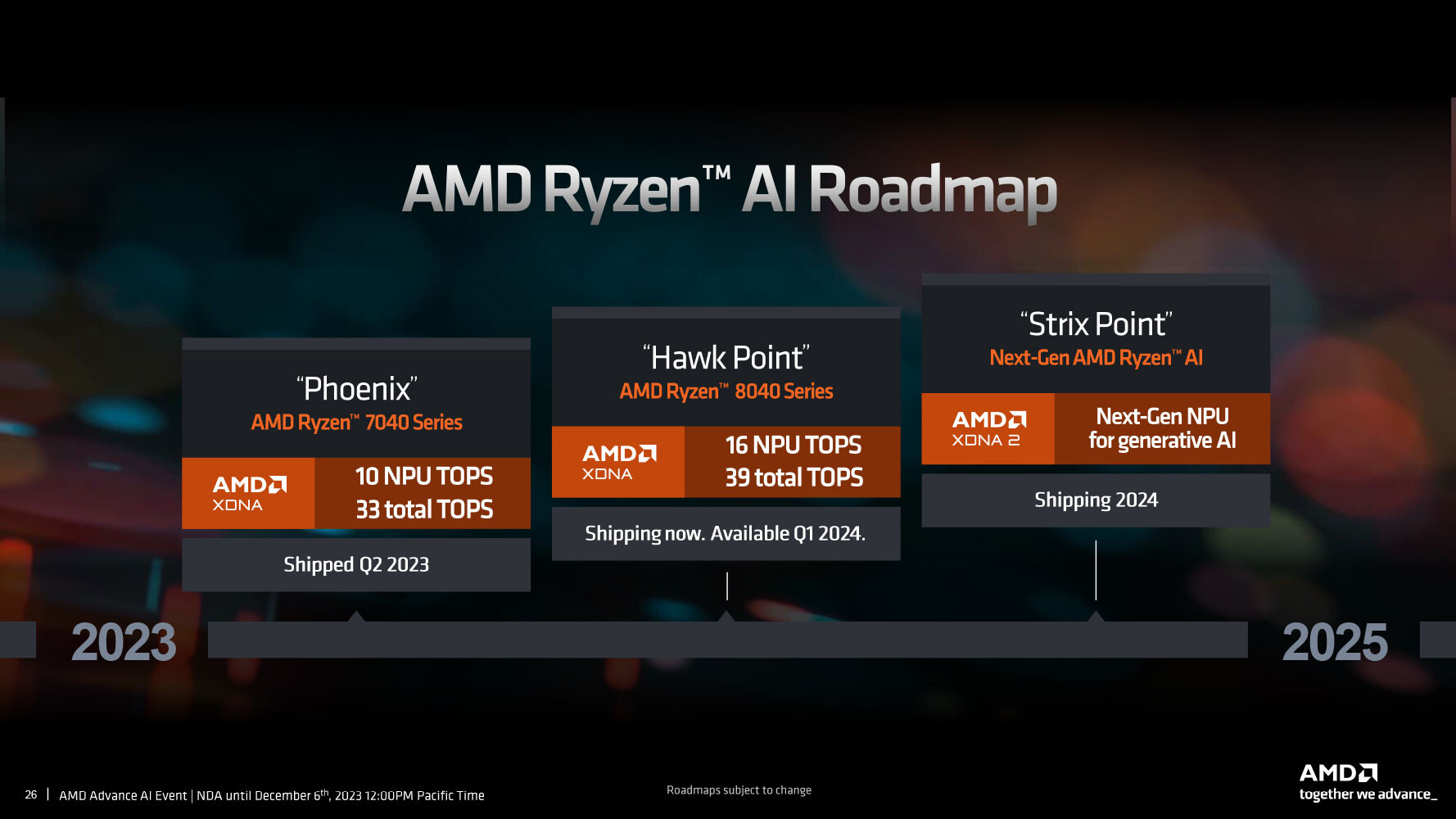
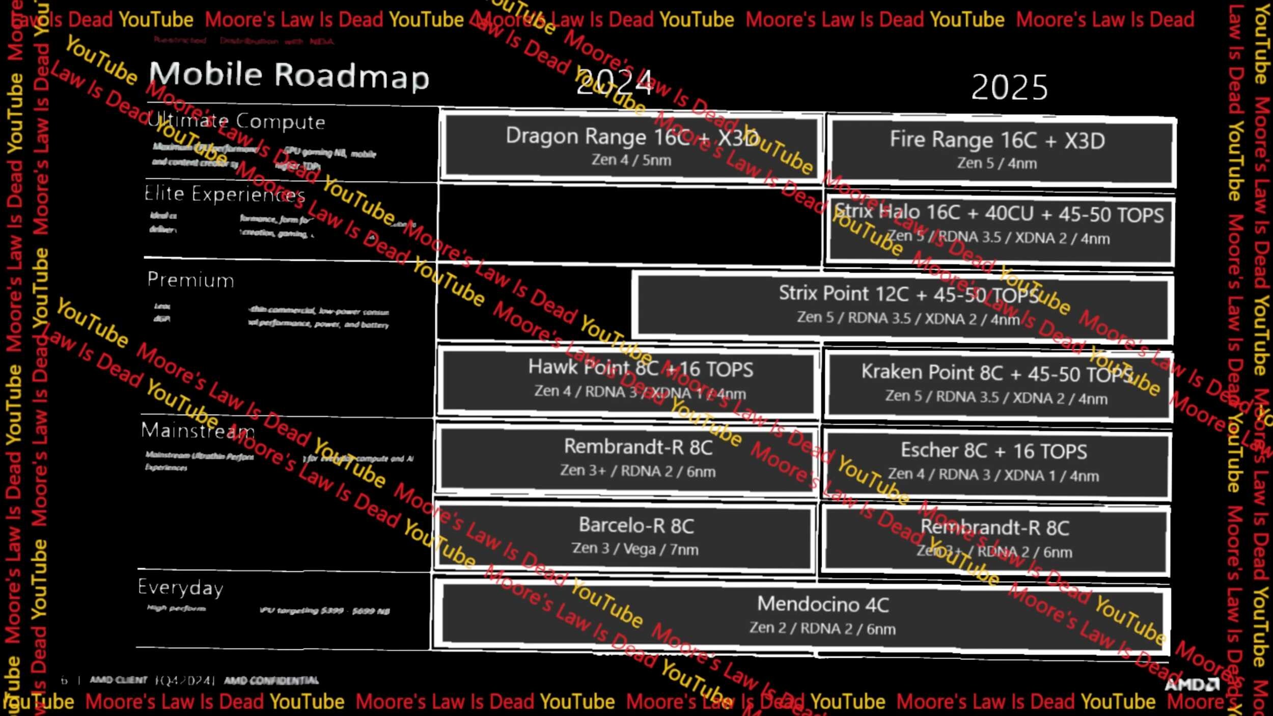
AMD "Strix Point" Mobile Processor Confirmed 12-core/24-thread, But Misses Out on PCIe Gen 5

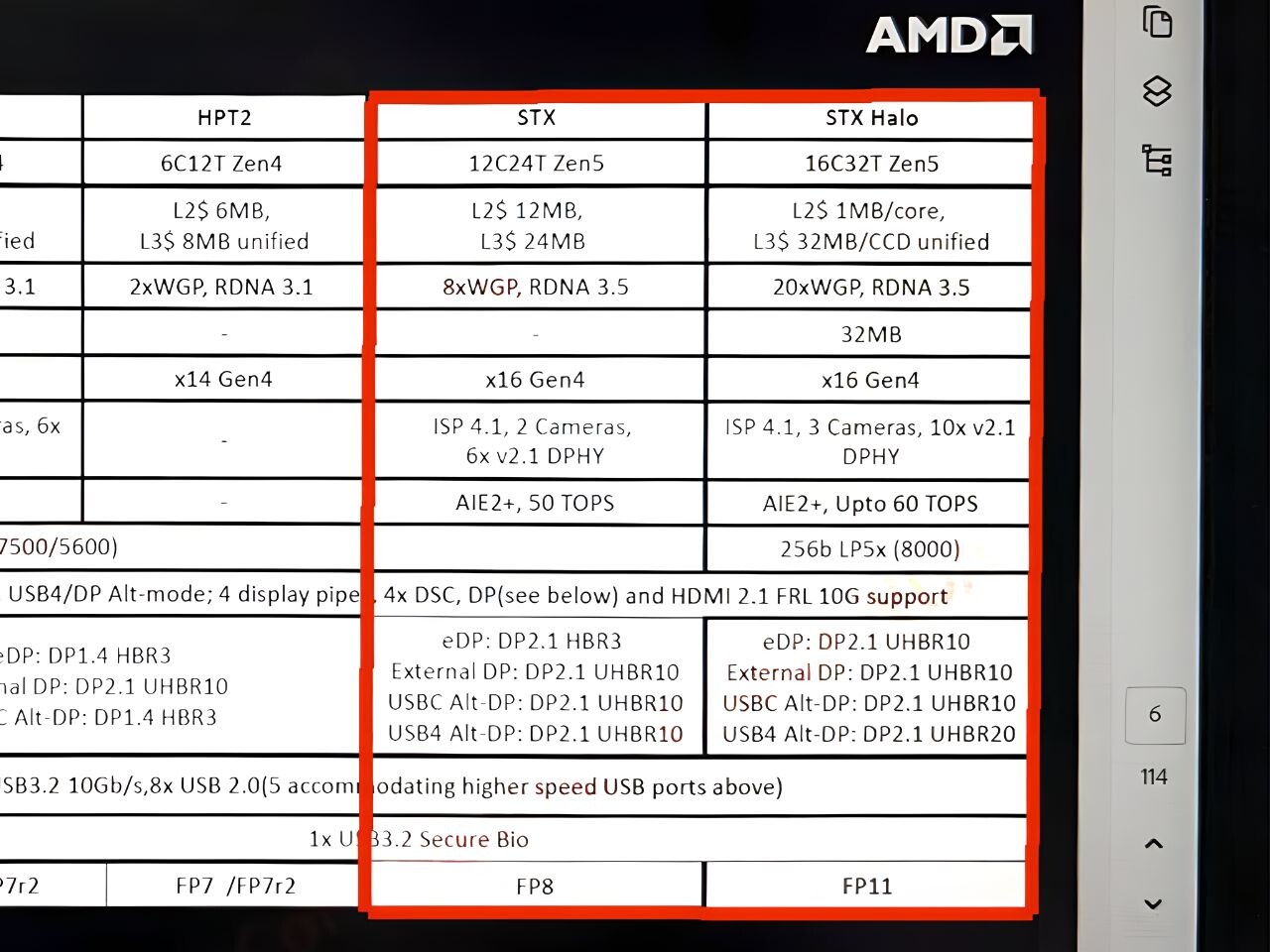
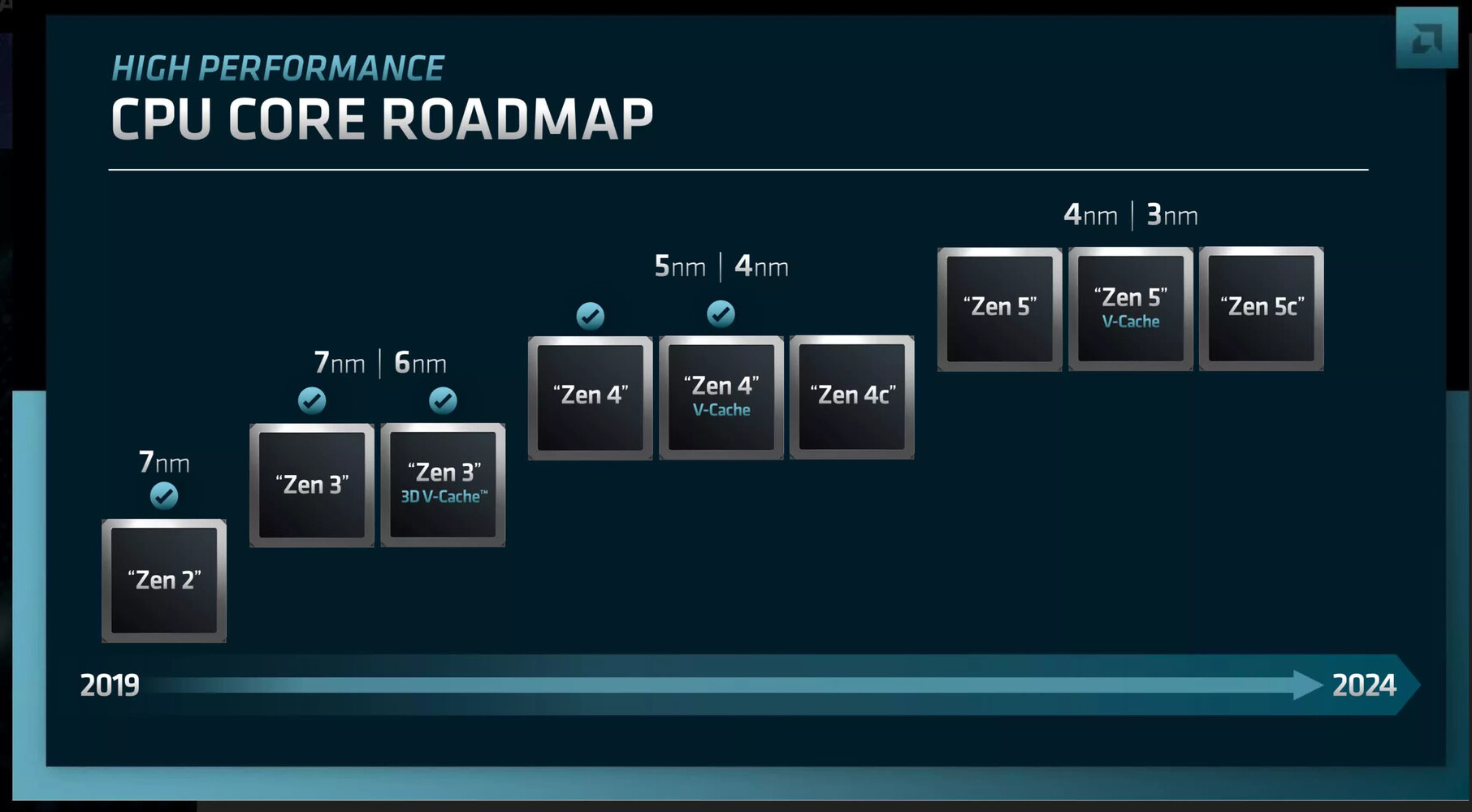
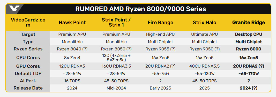
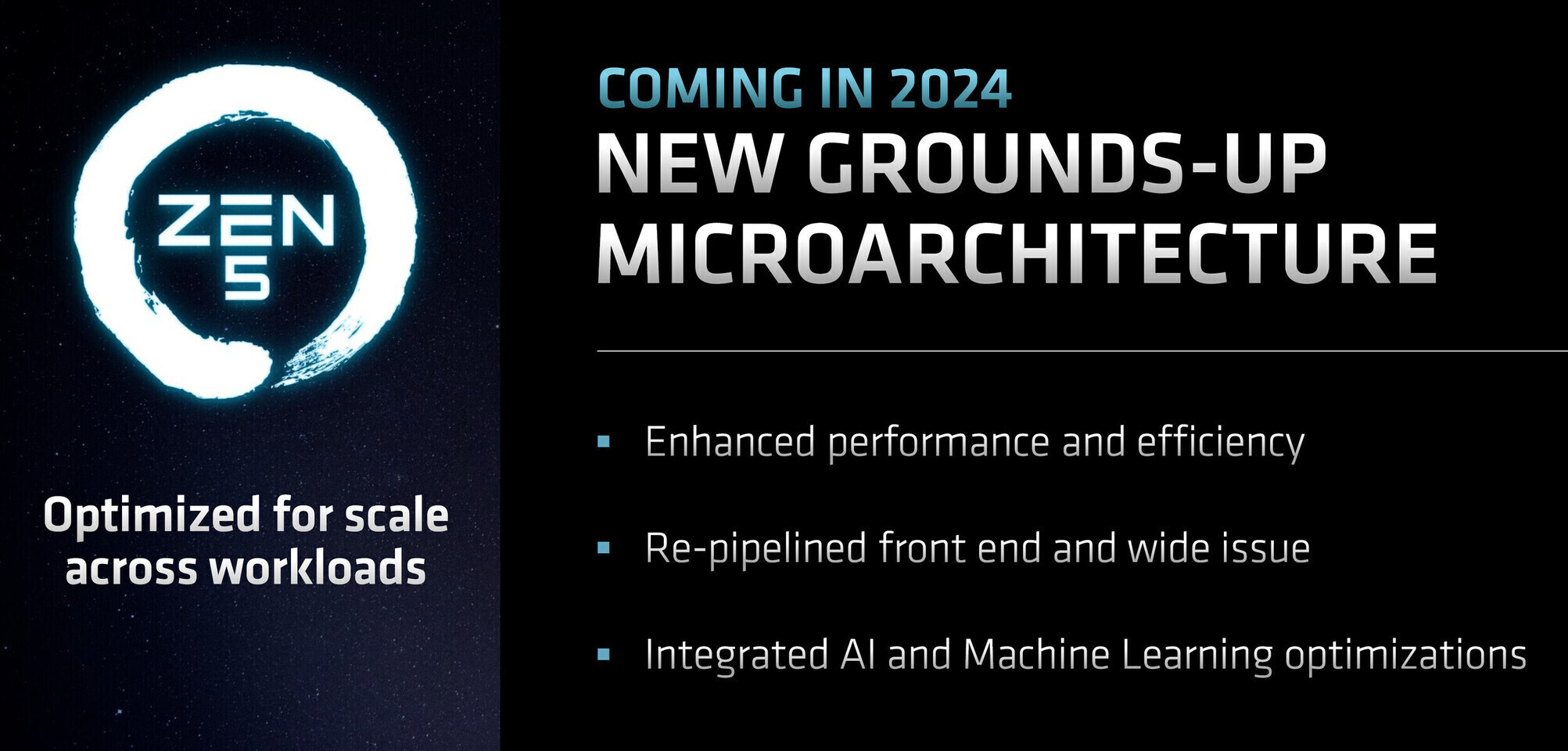
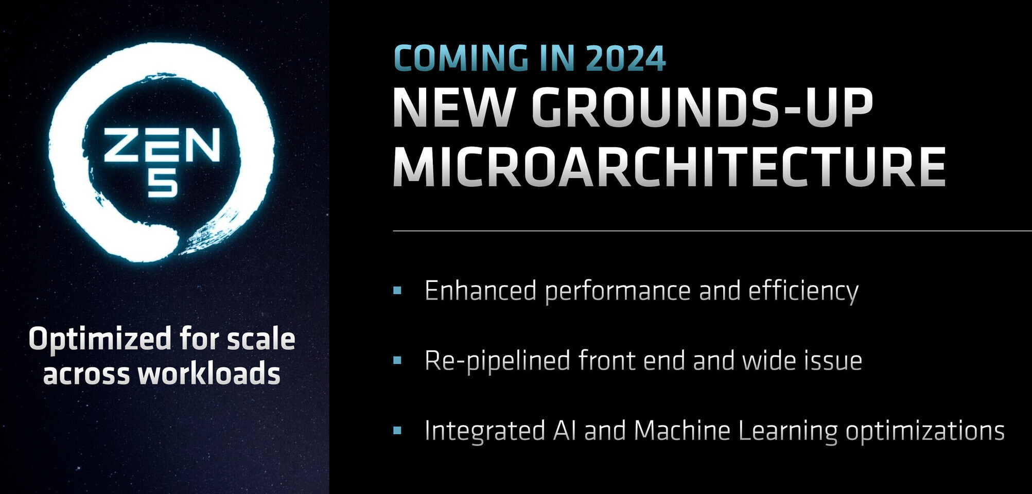
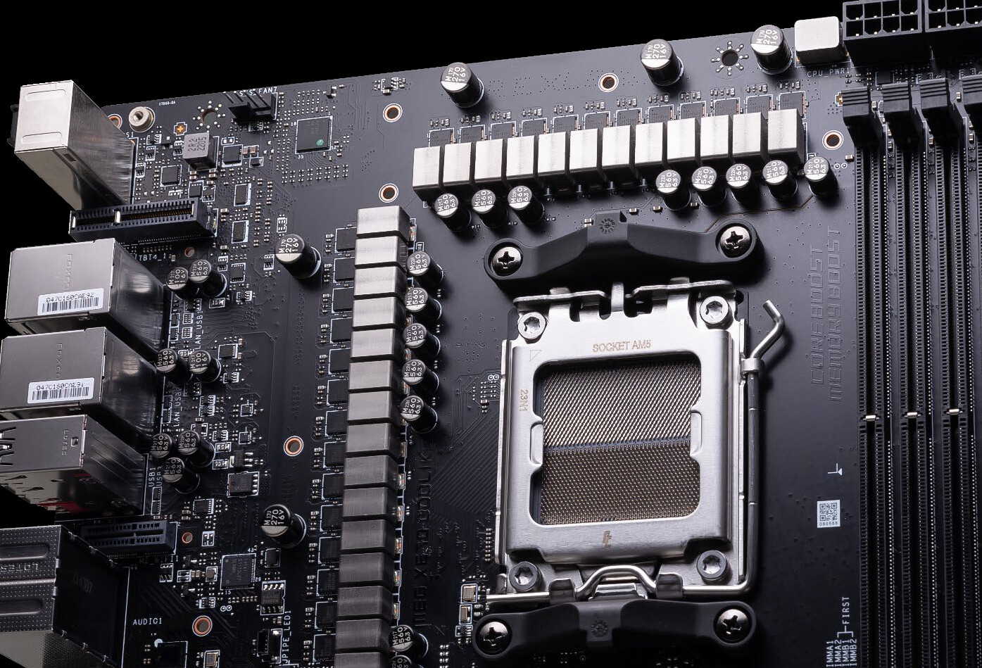
AMD's next-generation Ryzen 9000 "Strix Point" mobile processor, which succeeds the current Ryzen 8040 "Hawk Point" and Ryzen 7040 "Phoenix," is confirmed to feature a CPU core-configuration of 12-core/24-thread, according to a specs-leak by HKEPC citing sources among notebook OEMs. It appears like Computex 2024 will be big for AMD, with the company preparing next-gen processor announcements across the desktop and notebook lines. Both the "Strix Point" mobile processor and "Granite Ridge" desktop processor debut the company's next "Zen 5" microarchitecture.

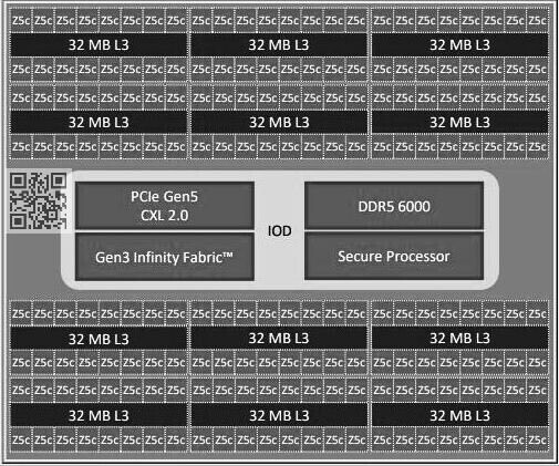
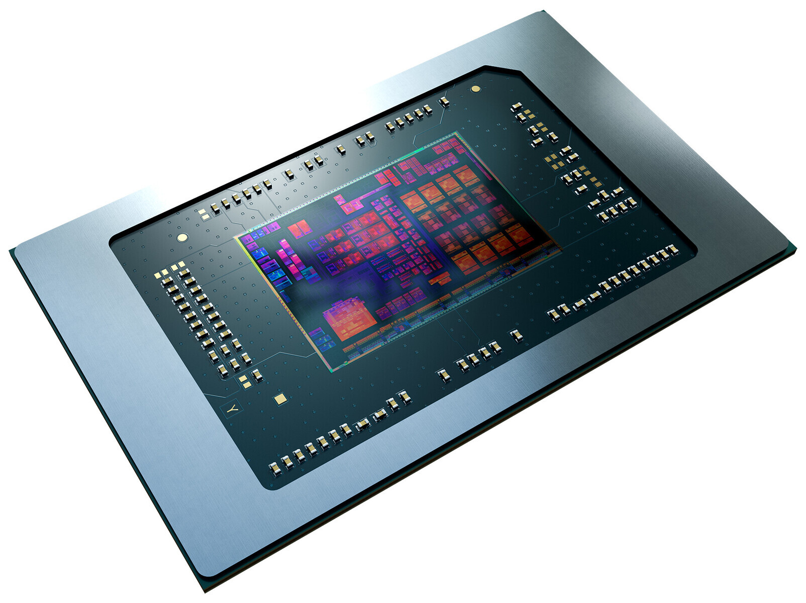
Perhaps the biggest takeaway from "Zen 5" is that AMD has increased the number of CPU cores per CCX from 8 in "Zen 3" and "Zen 4," to 12 in "Zen 5." While this doesn't affect the core-counts of its CCD chiplets (which are still expected to be 8-core), the "Strix Point" processor appears to use one giant CCX with 12 cores. Each of the "Zen 5" cores has a 1 MB dedicated L2 cache, while the 12 cores share a 24 MB L3 cache. The 12-core/24-thread CPU, besides the generational IPC gains introduced by "Zen 5," marks a 50% increase in CPU muscle over "Hawk Point." It's not just the CPU complex, even the iGPU sees a hardware update.

AMD "Strix Halo" Zen 5 Mobile Processor Pictured: Chiplet-based, Uses 256-bit LPDDR5X

Enthusiasts on the ChipHell forum scored an alleged image of AMD's upcoming "Strix Halo" mobile processor, and set out to create some highly plausible schematic slides. These are speculative. While "Strix Point" is the mobile processor that succeeds the current "Hawk Point" and "Phoenix" processors; "Strix Halo" is in a category of its own—to offer gaming experiences comparable to discrete GPUs in the ultraportable form-factor where powerful discrete GPUs are generally not possible. "Strix Halo" also goes head on against Apple's M3 Max and M3 Pro processors powering the latest crop of MacBook Pros. It has the same advantages as a single-chip solution, as the M3 Max.

The "Strix Halo" silicon is a chiplet-based processor, although very different from "Fire Range". The "Fire Range" processor is essentially a BGA version of the desktop "Granite Ridge" processor—it's the same combination of one or two "Zen 5" CCDs that talk to a client I/O die, and is meant for performance-thru-enthusiast segment notebooks. "Strix Halo," on the other hand, use the same one or two "Zen 5" CCDs, but with a large SoC die featuring an oversized iGPU, and 256-bit LPDDR5X memory controllers not found on the cIOD. This is key to what AMD is trying to achieve—CPU and graphics performance in the league of the M3 Pro and M3 Max at comparable PCB and power footprints.

MSI First with Motherboard BIOS that Supports Ryzen 9000 "Zen 5" Processors

In yet another clear sign that we could see some action from AMD on the next-gen desktop processor front this Computex, motherboard maker MSI released its first beta UEFI firmware update that packs an AGESA microcode that reportedly supports the upcoming AMD Ryzen 9000 "Granite Ridge" processors. The "7D74v1D2 beta" firmware update for the MSI MPG B650 Carbon Wi-Fi motherboard encapsulates AGESA ComboPI 1.1.7.0 patch-A, with the description that it supports a "next-gen CPU," a reference to the Ryzen 9000 "Granite Ridge."

A successor to the Ryzen 7000 Raphael, the Ryzen 9000 Granite Ridge introduces the new "Zen 5" microarchitecture to the desktop platform, with CPU core counts remaining up to 16-core/32-thread. The new microarchitecture is expected to introduce generational increase in IPC, as well as improve performance of certain exotic workloads such as AVX-512. The processors are said to be launching alongside the new AMD 800-series motherboard chipset. If AMD is using Computex as a platform to showcase these processors, it's likely we might see the first of these motherboards as well.

AMD Ryzen 9000 "Granite Ridge" Zen 5 Processor Pictured

An alleged picture of an unreleased AMD Ryzen 9000 series "Granite Ridge" desktop processor, just hit the wires. "Granite Ridge" is codename for the desktop implementation of the "Zen 5" microarchitecture, it succeeds the current Ryzen 7000 "Raphael" that's powered by "Zen 4." From what we're hearing, the CPU core counts of "Granite Ridge" continue to top out at 16. These chips will be built in the existing AMD Socket AM5 package, and will be compatible with existing AMD 600-series chipset motherboards, although the company is working on a new motherboard chipset to go with the new chips.

The alleged AMD engineering sample pictured below has an OPN 100-000001290-11, which is unreleased. This OPN also showed up on an Einstein@Home online database, where the distributed computing platform read it as having 16 threads, making this possibly an 8-core/16-thread SKU. The "Zen 5" microarchitecture is expected to provide a generational IPC increase over "Zen 4," but more importantly, offer a significant performance increase for AVX-512 workloads due to an updated FPU. AMD is expected to unveil its Ryzen 9000 series "Zen 5" processors at the 2024 Computex.

AMD Zen 5 Execution Engine Leaked, Features True 512-bit FPU

AMD "Zen 5" CPU microarchitecture will introduce a significant performance increase for AVX-512 workloads, with some sources reported as high as 40% performance increases over "Zen 4" in benchmarks that use AVX-512. A Moore's Law is Dead report detailing the execution engine of "Zen 5" holds the answer to how the company managed this—using a true 512-bit FPU. Currently, AMD uses a dual-pumped 256-bit FPU to execute AVX-512 workloads on "Zen 4." The updated FPU should significantly improve the core's performance in workloads that take advantage of 512-bit AVX or VNNI instructions, such as AI.

Giving "Zen 5" a 512-bit FPU meant that AMD also had to scale up the ancillaries—all the components that keep the FPU fed with data and instructions. The company therefore increased the capacity of the L1 DTLB. The load-store queues have been widened to meet the needs of the new FPU. The L1 Data cache has been doubled in bandwidth, and increased in size by 50%. The L1D is now 48 KB in size, up from 32 KB in "Zen 4." FPU MADD latency has been reduced by 1 cycle. Besides the FPU, AMD also increased the number of Integer execution pipes to 10, from 8 on "Zen 4." The exclusive L2 cache per core remains 1 MB in size.
Update 07:02 UTC: Moore's Law is Dead reached out to us and said that the slide previously posted by them, which we had used in an earlier version of this article, is fake, but said that the information contained in that slide is correct, and that they stand by the information.

Alleged AMD Ryzen "Granite Ridge" Engineering Samples Pop Up in Shipping Manifests

Shipping manifests appear to be great sources of pre-release information—only a few hours ago, the existence of prototype AMD "Strix Point" and "Fire Range" mobile processors was highlighted by hardware sleuth harukaze5719. A related leak has appeared online fairly quickly after the discovery of laptop-oriented "Zen 5" chips. momomo_us joined in on the fun, with their exposure of speculated desktop silicon. Two brand-new AMD OPN codes have been linked to the upcoming "Granite Ridge" series of AM5 processors.

100-000001404-01 is likely an eight-core/ sixteen-thread "Zen 5" Ryzen CPU with a 170 W TDP—a stepping designation, B0, indicates engineering sample status. The other listing, 100-000001290-21, seems to be an A0-type engineering sample—leaked info suggests that this a six-core/twelve-thread (105 W TDP) next-gen mainstream desktop processor. AMD is likely nearing the finish line with its Ryzen 9000-series—a new generation of chipsets, including X870E, is reportedly in the pipeline. Additionally, VideoCardz posits that a refresh of 700-series boards could be on the cards. "Granite Range" CPUs are expected to retain the current-gen 6 nm client I/O die (cIOD), as sported by "Raphael" Ryzen 7000-series desktop processors.

AMD "Zen 5" Based "Strix Point" and "Fire Range" Mobile Processors Spied in Shipping Manifests

Two of AMD's upcoming mobile processors that implement the "Zen 5" microarchitecture, "Strix Point" and "Fire Range," were spotted in shipping manifests. These are prototypes moving between AMD and its OEM partners. The manifest explicitly mentions a "Fire Range" 16-core processor sample with 55 W TDP, another "Fire Range" chip with an 8-core configuration and the same 55 W power; and a trio of "Strix Point" processors with a 28 W power design. Two of these are Ryzen 9 SKUs, and one of them is a Ryzen 7.

VideoCardz has the OPN codes for the samples being moved. The Ryzen 7 "Strix Point" sample bears 100-0000001335. One of the two Ryzen 9 "Strix Point" chips bears 100-000000994. The 16-core "Fire Range" is marked 100-000001028, while the 8-core "Fire Range" is 100-000001029. "Strix Point" will be AMD's most imporant mobile processor silicon, as this will be the one with a "Zen 5" CPU core count relevant to the notebook market, pack an RDNA 3+ iGPU, and that alleged 40 TOPS+ XDNA 2 NPU that can run Microsoft Copilot locally. A step up from this will be "Strix Halo," with a higher CPU core count, a much larger iGPU designed for performance-segment gaming. "Fire Range" is essentially a low Z-height BGA version of the "Granite Ridge" chiplet processor that has up to two "Zen 5" CCDs and an I/O die.

AMD EPYC "Turin" 9000-series Motherboard Specs Suggest Support for DDR5 6000 MT/s

AMD's next-gen EPYC Zen 5 processor family seems to be nearing launch status—late last week, momomo_us uncovered an unnamed motherboard's datasheet; this particular model will accommodate a single 9000-series CPU—with a maximum 400 W TDP—via an SP5 socket. 500 W and 600 W limits have been divulged (via leaks) in the past, so the 400 W spec could be an error or a: "legitimate compatibility issue with the motherboard, though 400 Watts would be in character with high-end Zen 4 SP5 motherboards," according to Tom's Hardware analysis.

AMD's current-gen "Zen 4" based EPYC "Genoa" processor family—sporting up to 96-cores/192-threads—is somewhat limited by its DDR5 support transfer rates of up to 4800 MT/s. The latest leak suggests that "Turin" is upgraded quite nicely in this area—when compared to predecessors—the SP5 board specs indicate DDR5 speeds of up to 6000 MT/s with 4 TB of RAM. December 2023 reports pointed to "Zen 5c" variants featuring (max.) 192-core/384-thread configurations, while larger "Zen 5" models are believed to be "modestly" specced with up to 128-cores and 256-threads. AMD has not settled on an official release date for its EPYC "Turin" 9000-series processors, but a loose launch window is expected "later in 2024" based on timeframes presented within product roadmaps.

AMD Roadmaps Next-gen Ryzen "Strix Point" CPUs at AI PC Summit

Dr. Lisa Su introduced AMD's "next-gen AMD Ryzen" processor series during a recent presentation at the Beijing AI PC Innovation Summit—this announcement confirms that Team Red's RDNA 3+ (AKA 3.5) graphics technology is destined to arrive (on board) with the launch of "Strix Point" processors. Product roadmaps remain unchanged—when compared to slides from last December—AMD still anticipates a 2024 launch window. China has been introduced to current-gen "Hawk Point" Ryzen 8040 mobile and 8000G (AM5) desktop processors—key AMD personnel presented a variety of products, including region-specific budget options.

David Wang, SVP of GPU Technology and Engineering R&D, covered the RDNA 3+ and XDNA 2 architectures (very briefly) during his on-stage appearance—he dedicated most of his attention to current-gen "Hawk Point" processors. The Strix Point integrated solution—a GFX1150 target—has been linked to "RDNA 3.5" for a while, a lot of this information was gleaned from publicly visible AMD patch notices. The latest Team Red software engineering activities indicate that Zen 5 CPU enablement is nearing a possible finish line.

AMD Zen 5 "Znver5" CPU Enablement Spotted in Change Notes

Close monitoring of AMD engineering activities—around mid-February time—revealed the existence of a new set of patches for GNU Compiler Collection (GCC). At the time, news reports put spotlights on Team Red's "znver5" enablement—this target indicated that staffers were prepping Zen 5 processor microarchitecture with an expanded AVX instruction set (building on top of Zen 4's current capabilities). Phoronix's Michael Larabel has fretted over AMD's relative silence over the past month—regarding a possible merging of support prior to the stable release of GCC 14.

He was relieved to discover renewed activity earlier today: "AMD Zen 5 processor enablement has been merged to GCC Git in time for the GCC 14.1 stable release that will be out in the coming weeks. It was great seeing AMD getting their Zen 5 processor enablement upstreamed ahead of any Ryzen or EPYC product launches and being able to do so in time for the annual major GNU Compiler Collection feature release." Team Red is inching ever closer to the much anticipated 2024 rollout of next-gen Ryzen 9000 processors, please refer to a VideoCardz-authored timeline diagram (below)—"Granite Ridge" is an incoming AM5 desktop CPU family (reportedly utilizing Zen 5 and RDNA 2 tech), while "Strix Point" is scheduled to become a mobile APU series (Zen 5 + RDNA 3.5).

Qubic Cryptocurrency Mining Craze Causes AMD Ryzen 9 7950X Stocks to Evaporate

It looks like cryptocurrency mining is back in craze, as miners are firing up their old mining hardware from 2022 to cash in. Bitcoin is now north of $72,000, and is dragging up the value of several other cryptocurrencies, one such being Qubic (QBIC). Profitability calculators put 24 hours of Qubic mining on an AMD Ryzen 9 7950X 16-core processor at around $3, after subtracting energy costs involved in running the chip at its default 170 W TDP. "Zen 4" processors such as the 7950X tend to retain much of their performance with slight underclocking, and reducing their power limits; which is bound to hold or increase profitability, while also prolonging the life of the hardware.

And thus, the inevitable has happened—stocks of the AMD Ryzen 9 7950X have disappeared overnight across online retail. With the market presence of the 7950X3D and the Intel Core i9-14900K, the 7950X was typically found between $550-600, which would have added great value considering its low input costs. CPU-based cryptocurrency miners, including the QBIC miner, appear to be taking advantage of the AVX-512 instruction set. AMD "Zen 4" microarchitecture supports AVX-512 through its dual-pumped 256-bit FPU, and the upcoming "Zen 5" microarchitecture is rumored to double AVX-512 performance over "Zen 4." Meanwhile, Intel has deprecated what few client-relevant AVX-512 instructions its Core processors had since 12th Gen "Alder Lake," as it reportedly affected sales of Xeon processors. What about the 7950X3D? It's pricier, but mining doesn't benefit from the 3D V-cache, and the chip doesn't sustain the kind of CPU clocks the 7950X manages to do across all its 16 cores. It's only a matter of time before the 7950X3D disappears, too; followed by 12-core models such as the 65 W 7900, the 170 W 7900X, and the 7900X3D.

AMD Pushes Performance Monitoring Patches for Upcoming Zen 5 CPUs

Thanks to Phoronix, we have discovered that AMD has recently released initial patches for performance monitoring and events related to their upcoming Zen 5 processors in the Linux kernel. These patches, sent out for review on the kernel mailing list, provide the necessary JSON files for PMU (Performance Monitoring Unit) events and metrics that will be exposed through the Linux perf tooling. As the patches consist of JSON additions and do not risk regressing existing hardware support, there is a possibility that they could be included in the upcoming Linux v6.9 kernel cycle. This would allow developers and enthusiasts to access detailed performance data for Zen 5 CPUs once they become available, helping with optimization and analysis of the next-generation processors.

The release of these patches follows AMD's publication of performance monitor counter documentation for AMD Family 1Ah Model 00h to 0Fh processors last week, confirming that these models represent the upcoming Zen 5 lineup. While Linux kernel 6.8 already includes some elements of Zen 5 CPU support, the upstream Linux enablement for these next-generation AMD processors is an ongoing process. Upon Phoronix examining the Zen 5 core and uncore events, as well as the metrics and mappings, it appears that they are mainly similar to those found in the current Zen 4 processors. This suggests that AMD has focused on refining and optimizing the performance monitoring capabilities of its new architecture rather than introducing significant changes. As the launch of Zen 5 CPUs draws closer, we await to see the performance and capabilities of these next-generation processors. With performance monitoring also getting a push, this could be a sign that Zen 5 launch is nearing.

AMD "Zen 5c" CCDs Made On More Advanced 3 nm Node Than "Zen 5"

AMD is reportedly building its upcoming "Zen 5" and "Zen 5c" CPU Core Dies (CCDs) on two different foundry nodes, a report by Chinese publication UDN, claims. The Zen 5 CCD powering the upcoming Ryzen "Granite Ridge" desktop processors, "Fire Range" mobile processors, and EPYC "Turin" server processors, will be reportedly built on the 4 nm EUV foundry node, a slightly more advanced node than the current 5 nm EUV the company is building "Zen 4" CCDs on. The "Zen 5c" CCD, or the chiplet with purely "Zen 5c" cores in a high density configuration; on the other hand, will be built on an even more advanced 3 nm EUV foundry node, the report says. Both CCDs will go into mass production in Q2-2024, with product launches expected across the second half of the year.

The "Zen 5c" chiplet has a mammoth 32 cores spread across two CCXs of 16 cores, each. Each CCX has 16 cores sharing a 32 MB L3 cache. It is to cram these 32 cores, each with 1 MB of L2 cache; and a total of 64 MB of L3 cache, that AMD could be turning to the 3 nm foundry node. Another reason could be voltages. If "Zen 4c" is anything to go by, the "Zen 5c" core is a highly compacted variant of "Zen 5," which operates at a lower voltage band than its larger sibling, without any change in IPC or instruction sets. The decision to go with 3 nm could be a move aimed at increasing clock speeds at those lower voltages, in a bid to generationally improve performance using clock speeds, besides IPC and core count. The EPYC processor with "Zen 5c" chiplets will feature no more than six such large CCDs, for a maximum core count of 192. The regular "Zen 5" CCD has just 8 cores in a single CCX, with 32 MB of L3 cache shared among the cores; and TSV provision for 3D Vertical Cache, to increase the L3 cache in special variants.

AMD Zen 5 Details Emerge with GCC "Znver5" Patch: New AVX Instructions, Larger Pipelines

AMD's upcoming family of Ryzen 9000 series of processors on the AM5 platform will carry a new silicon SKU under the hood—Zen 5. The latest revision of AMD's x86-64 microarchitecture will feature a few interesting improvements over its current Zen 4 that it is replacing, targeting the rumored 10-15% IPC improvement. Thanks to the latest set of patches for GNU Compiler Collection (GCC), we have the patch set that proposes changes taking place with "znver5" enablement. One of the most interesting additions to the Zen 5 over the previous Zen 4 is the expansion of the AVX instruction set, mainly new AVX and AVX-512 instructions: AVX-VNNI, MOVDIRI, MOVDIR64B, AVX512VP2INTERSECT, and PREFETCHI.

AVX-VNNI is a 256-bit vector version of the AVX-512 VNNI instruction set that accelerates neural network inferencing workloads. AVX-VNNI delivers the same VNNI instruction set for CPUs that support 256-bit vectors but lack full 512-bit AVX-512 capabilities. AVX-VNNI effectively extends useful VNNI instructions for AI acceleration down to 256-bit vectors, making the technology more efficient. While narrow in scope (no opmasking and extra vector register access compared to AVX-512 VNNI), AVX-VNNI is crucial in spreading VNNI inferencing speedups to real-world CPUs and applications. The new AVX-512 VP2INTERSECT instruction is also making it in Zen 5, as noted above, which has been present only in Intel Tiger Lake processor generation, and is now considered deprecated for Intel SKUs. We don't know the rationale behind this inclusion, but AMD sure had a use case for it.

AMD Readies X870E Chipset to Launch Alongside First Ryzen 9000 "Granite Ridge" CPUs

AMD is readying the new 800-series motherboard chipset to launch alongside its next-generation Ryzen 9000 series "Granite Ridge" desktop processors that implement the "Zen 5" microarchitecture. The chipset family will be led by the AMD X870E, a successor to the current X670E. Since AMD isn't changing the CPU socket, and this is very much the same Socket AM5, the 800-series chipset will support not just "Granite Ridge" at launch, but also the Ryzen 7000 series "Raphael," and Ryzen 8000 series "Hawk Point." Moore's Law is Dead goes into the details of what sets the X870E apart from the current X670E, and it all has to do with USB4.

Apparently, motherboard manufacturers will be mandated to include 40 Gbps USB4 connectivity with AMD X870E, which essentially makes the chipset a 3-chip solution—two Promontory 21 bridge chips, and a discrete ASMedia ASM4242 USB4 host controller; although it's possible that AMD's QVL will allow other brands of USB4 controllers as they become available. The Ryzen 9000 series "Granite Ridge" are chiplet based processors just like the Ryzen 7000 "Raphael," and while the 4 nm "Zen 5" CCDs are new, the 6 nm client I/O die (cIOD) is largely carried over from "Raphael," with a few updates to its memory controller. DDR5-6400 will be the new AMD-recommended "sweetspot" speed; although AMD might get its motherboard vendors to support DDR5-8000 EXPO profiles with an FCLK of 2400 MHz, and a divider.

AMD "Kraken Point" Silicon Succeeds "Hawk Point" with Zen 5 4P+4C Core Config, NPU

AMD's next generation Ryzen mobile processor family is undergoing a significant re-positioning of IP within its product stack, as the company introduces the new "elite experience" segment. The "Fire Range" mobile processor is a direct successor to "Dragon Range" MCM, with two 8-core "Zen 5" chiplets. It is essentially a BGA package of the desktop "Granite Ridge" processor, and comes with up to 16 "Zen 5" cores, for flagship gaming notebooks and mobile workstations. A segment below the current "Dragon Range" is the current "Hawk Point" silicon, driving premium experiences. There is a rather large CPU performance gap between the two, as would be the case between the upcoming "Fire Range" and "Kraken Point," which is why AMD is creating the "elite experience" segment, and filling it with "Strix Halo" and "Strix Point," which will square off against Core Ultra 7 and Core Ultra 9 processors, as well as certain HX-segment 14th Gen Core mobile processors. "Strix Point" has a significant core-count increase to 12, along with a large iGPU. We've extensively covered "Strix Point" in our older article, but now we have more information on the elusive "Kraken Point."

"Kraken Point" is codename for AMD's next-generation monolithic mobile processor silicon being designed to power Ryzen processor SKUs competing against the bulk of Intel Core Ultra 5 and Core Ultra 7 SKUs. This chip will be built on a refined 4 nm EUV node by TSMC, and will be monolithic. Its most interesting aspect is the CPU complex. It reportedly features a combination of four regular "Zen 5" cores, and four "Zen 5c" low power cores. All eight cores will likely share a single CCX, which means they share a common L3 cache, which enables easy movement of threads between the two kinds of cores, without having to make round-trips to the DRAM.

Tipster Claims AMD "Kraken Point" APU Configured with Zen 5 & Zen 5c Cores

Everest (@Olrak29_) has kept track of many AMD processor families over the past couple of years—his latest insight provides an early look at the alleged internal makeup of Team Red's "Kraken Point" APU series. The rumor mill has designated these next-gen mobile processors as 2025 follow-ups to the recently launched Ryzen 8040 "Hawk Point" family of mainstream laptop APUs. The tipster's initial social media post only mentioned the presence of both Zen 5 and Zen 5c cores within Kraken Point processors, but he later clarified that a total of eight cores would include four large units and four smaller types. TPU's past coverage of Kraken Point pointed to rumors of an 8-core, 16-thread configuration, but leaked slides (from late 2023) did not mention the integration of efficiency-tuned Zen 5c "Prometheus" cores, along with presumed Zen 5 "Nirvana" cores.

Everest's continuous flow of insider information reveals that "Kraken Point" shares many "Hawk Point" traits—four workgroup processors (WGP) could be present on final retail products, granting eight compute units (8 CUs in total). He responded to a query regarding AMD's choice of integrated graphics technology—the succinct answer being RDNA 3.5. Past leaks allege that XDNA 2 will drive the NPU side of things—offering a performance range of around 45 to 50 TOPS. The Kraken Point APU is believed to be sticking with a safe monolithic die design, manufactured on a non-specific 4 nm process. Team Red is rumored to be in TSMC's order books for all sorts of next generation silicon.

More AMD Ryzen 9000 "Zen 5" Desktop Processor Details Emerge

AMD is looking to debut its Ryzen 9000 series "Granite Ridge" desktop processors based on the "Zen 5" microarchitecture some time around May-June 2024, according to High Yield YT, a reliable source with AMD leaks. These processors will be built in the existing Socket AM5 package, and be compatible with all existing AMD 600 series chipset motherboards. It remains to be seen if AMD debuts a new line of motherboard chipsets. Almost all Socket AM5 motherboards come with the USB BIOS flashback feature, which means motherboards from even the earliest production batches that are in the retail channel, should be able to easily support the new processors.

AMD is giving its next-gen desktop processors the Ryzen 9000 series processor model numbering, as it used the Ryzen 8000 series for its recently announced Socket AM5 desktop APUs based on the "Hawk Point" monolithic silicon. "Granite Ridge" will be a chiplet-based processor, much like the Ryzen 7000 series "Raphael." In fact, it will even retain the same 6 nm client I/O die (cIOD) as "Raphael," with some possible revisions made to increase its native DDR5 memory frequency (up from the current DDR5-5200), and improve its memory overclocking capabilities. It's being reported that DDR5-6400 could be the new "sweetspot" memory speed for these processors, up from the current DDR5-6000.

AMD Zen 5 "Granite Ridge" CPUs Reportedly in Mass Production

AMD concentrated on the promotion of new Zen 4-based APU products at last week's CES trade show, and they even lobbed in a couple of new Zen 3 offerings for PC enthusiasts who are more than happy to stick with Team Red's last generation AM4 socket. Future-focused folks were a little bit disappointed with Team Red keeping quiet about their next-generation "Zen 5" CPUs at CES 2024—one seeker of information, Peter Weltzmaier, turned to a notorious source of hardware leaks on X. Kepler has a decent track record of providing accurate inside tracks—and they more than happy to address Weltzmaier's query regarding the status of AMD's upcoming "Granite Ridge" desktop CPU series.

Kepler believes that Granite Ridge has reached the mass production phase, but did not provide any further elaboration beyond a brief reply on social media—this information should be taken with a grain of salt. We have not heard a lot about Granite Ridge processors since last November, with AMD choosing to not preview next-gen desktop processors at a December "Advancing AI" event. The rumor mill proposed that XDNA-based Ryzen AI acceleration will not be a key feature present on Granite Ridge and a mobile-oriented derivative called "Fire Ridge."

AMD Zen 5 Linux Kernel Patches Point to Power Management Updates

AMD released its latest PMC (power management controller) driver patches for the Linux kernel, which reference a yet unreleased "Family 1Ah" processors. Phoronix believes this is the first reference to AMD's next generation "Zen 5" microarchitecture in the PMC driver. We've already seen AMD EPYC "Turin" server processors based on "Zen 5" in the flesh, and it's likely that AMD is handing these out to some of its biggest data-center customers for testing and evaluation, before giving them some final touches and green-lighting mass-production in 2024. The patches themselves are barely two new lines of code, and talk about a new sleep state called "s2idle." This is a software-defined system sleep state. The EPYC "Turin" processor comes in two packages, one with up to 128 "Zen 5" cores, and another with up to 192 "Zen 5c" cores for cloud applications.

AMD to Support AM5 Platform with New Products Till 2025 and Beyond

AMD continues to release new Ryzen 5000 series processor models for the Socket AM4 platform to this day, with new processors expected to launch next month. That's over 6 years of longevity for the platform, considering that AMD has extended official Ryzen 5000 series support all the way back to its first line of AM4 motherboards based on the 300-series chipset. The company plans a similar longevity for Socket AM5. In an interview with Overclockers UK, AMD's client channel business head David McAfee said "I think that we certainly recognized that the longevity of the AM4 platforms was one of the biggest reasons that led to the success of Ryzen and as we think and as we think about the future, 2025 and beyond, that decision to move to a next-generation of socket is one that's going to be really thought through really really carefully. We know the impact that moving to a new socket brings and we want to stay on AM5 for as long as we possibly can. We are firmly committed to 2025 and beyond and we will see how long that promise lasts beyond 2025."

AMD Socket AM5 is designed to deliver up to 230 W of package power, and has a contemporary I/O that includes a dual-channel DDR5 memory interface (4x 40-bit sub-channels); and 28 PCIe Gen 5 lanes (x16 PEG, two x4 NVMe, and x4 chipset bus), besides the usual SoC connectivity. With the upcoming Ryzen 8000G "Phoenix" APUs, we could expect to see that the socket even wires out modern display I/O such as DisplayPort 2.1 with USB type-C, and the bandwidth for 12-bit HDR up to 68 billion colors. AMD debuted Socket AM5 with the "Zen 4" microarchitecture, with "Zen 5" expected to launch in 2024. It's conceivable that the company's 2025 client architecture, "Zen 6," could also see its desktop presence on AM5, given that DDR5 memory and PCIe Gen 5 will remain relevant till at least that time.

AMD 5th Gen EPYC "Turin" Pictured: Who Needs Accelerators When You Have 192 Cores?

AMD's upcoming server processor, the 5th Gen EPYC "Turin," has been pictured as an engineering sample is probably being evaluated by the company's data-center or cloud customers. The processor has a mammoth core-count of 192-core/384-thread in its high-density cloud-focused variant that uses "Zen 5c" CPU cores. Its regular version that uses larger "Zen 5" cores that can sustain higher clock speeds, also comes with a fairly high core-count of 128-core/256-thread, up from the 96-core/192-thread of the "Zen 4" based EPYC "Genoa."

The EPYC "Turin" server processor based on "Zen 5" comes with an updated sIOD (server I/O die), surrounded by as many as 16 CCDs (CPU complex dies). AMD is expected to build these CCDs on the TSMC N4P foundry node, which is a more advanced version of the TSMC N4 node the company currently uses for its "Phoenix" client processors, and the TSMC N5 node it uses for its "Zen 4" CCD. TSMC claims that the N4P node offers an up to 22% improvement in power efficiency over N5, as well as a 6% increase in transistor density. Each of the "Zen 5" CCDs is confirmed to have 8 CPU cores sharing 32 MB L3 cache memory. A total of 16 such CCDs add up to the processor's 128-core/256-thread number. The high-density "Turin" meant for cloud data-centers, is a whole different beast.

AMD Announces XDNA 2 NPU Architecture for Next Gen "Strix Point" Mobile Processors Arriving in 2024

AMD in its Ryzen 8040 series "Hawk Point" mobile processors announcement made the first mention of XDNA 2, its next-generation on-chip neural processing unit (NPU) architecture. Above all, the XDNA 2 NPU is expected to introduce an over 3 times improvement in performance over the first generation XDNA NPU powering the Ryzen 7040 series "Phoenix" processor. XDNA 2 is making its debut with AMD's next-generation Ryzen "Strix Point" mobile processor that the company looks to launch in 2024. While "Phoenix" offers 10 TOPS of NPU performance, AMD mentions an "over 3 times" performance improvement, which probably puts this figure at 32 TOPS for "Strix Point."

The "Strix Point" mobile processor is rumored to debut faster "Zen 5" CPU cores, a possible CPU core count increase to 12, and a much more powerful iGPU based on the updated RDNA 3.5 graphics architecture, with some SKUs expected to feature CU counts as high as 32, and designed to square off against the iGPU of the Apple M3 Max processor. Besides "Zen 5" CPU cores and RDNA 3.5 iGPU, we now know that even the NPU gets an overhaul with this XDNA 2 announcement, and a possible 32 TOPS NPU performance.

Leaked Flyer Hints at Possible AMD Ryzen 9000 Series Powered by Zen 5

A curious piece of marketing material on the Chiphell forum has sent ripples through the tech community, featuring what appears to be an Alienware desktop equipped with an unannounced AMD Ryzen 9000-series processor. The authenticity of this flyer is up for debate, with possibilities ranging from a simple typo by Alienware to a fabricated image, or it could even suggest that AMD is on the cusp of unveiling its next-generation Ryzen CPUs for desktop PCs. While intrigue is high, it's important to approach such revelations cautiously, with a big grain of salt. AMD's existing roadmap points toward a 2024 release for its Zen 5-based Ryzen desktop processors and EPYC server CPUs, which casts further doubt on the Ryzen 9000 series appearing ahead of schedule.

We have to wait for AMD's major upcoming events, including the "Advancing AI" event on December 6, where the company will showcase how its partners and AMD use AI for applications. Next, we hope to hear from AMD about upcoming events such as CES in January and Computex in May, but we don't have any official information on product launches in the near term. If the company is preparing anything, the Alienware flyer pictured below should indicate it, if the source is confirmed. However, the doubt remains, and we should be skeptical of its truthfulness.

AMD Mobile Processor Lineup in 2025 Sees "Fire Range," "Strix Halo," and Signficant AI Performance Increases

With Windows 11 23H2 setting the stage for increased prevalence of AI in client PC use cases, the new hardware battleground between AMD and its rivals Intel, Apple, and Qualcomm, will be in equipping their mobile processors with sufficient AI acceleration performance. AMD already introduced accelerated AI with the current "Phoenix" processor that debuts Ryzen AI, and its Xilinx XDNA hardware backend that provides a performance of up to 16 TOPS. This will see a 2-3 fold increase with the company's 2024-25 mobile processor lineup, according to a roadmap leak by "Moore's Law is Dead."

At the very top of the pile, in a product segment called "ultimate compute," which consists of large gaming notebooks, mobile workstations, and desktop-replacements; the company's current Ryzen 7045 "Dragon Range" processor will continue throughout 2024. Essentially a non-socketed version of the desktop "Raphael" MCM, "Dragon Range" features up to two 5 nm "Zen 4" CCDs for up to 16 cores, and a 6 nm cIOD. This processor lacks any form of AI acceleration. In 2025, the processor will be succeeded with "Fire Range," a similar non-socketed, mobile-friendly MCM that's derived from "Granite Ridge," with up to two 4 nm "Zen 5" CCDs for up to 16 cores; and the 6 nm cIOD. What's interesting to note here, is that the quasi-roadmap makes no mention of AI acceleration for "Fire Range," which means "Granite Ridge" could miss out on Ryzen AI acceleration from the processor. Modern discrete GPUs from both NVIDIA and AMD support AI accelerators, so this must have been AMD's consideration to exclude an XDNA-based Ryzen AI accelerator on "Fire Range" and "Granite Ridge."
Return to Keyword Browsing
Apr 29th, 2024 18:52 EDT change timezone

New Forum Posts

Popular Reviews

Controversial News Posts