News Posts matching #layers

Return to Keyword Browsing

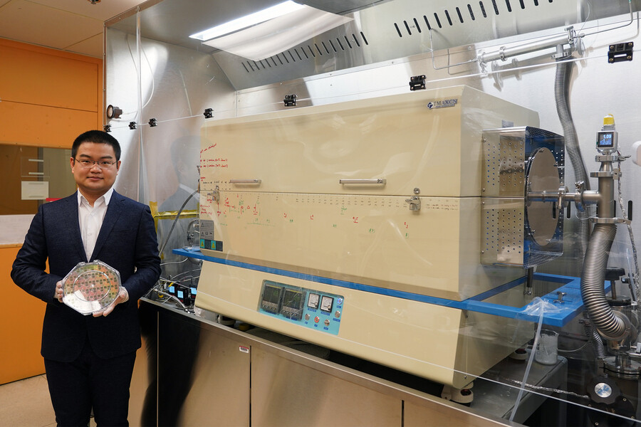
Kioxia and WD Elevate Capacity Utilization, Pushing NAND Flash Supply Growth to 10.9%

TrendForce reports that anticipation of NAND Flash price hikes into Q2 has motivated certain suppliers to minimize losses and lower costs in hopes of returning to profitability this year. Kioxia and WD led the charge from March, boosting their capacity utilization rates to nearly 90%—a move not widely adopted by their competitors.

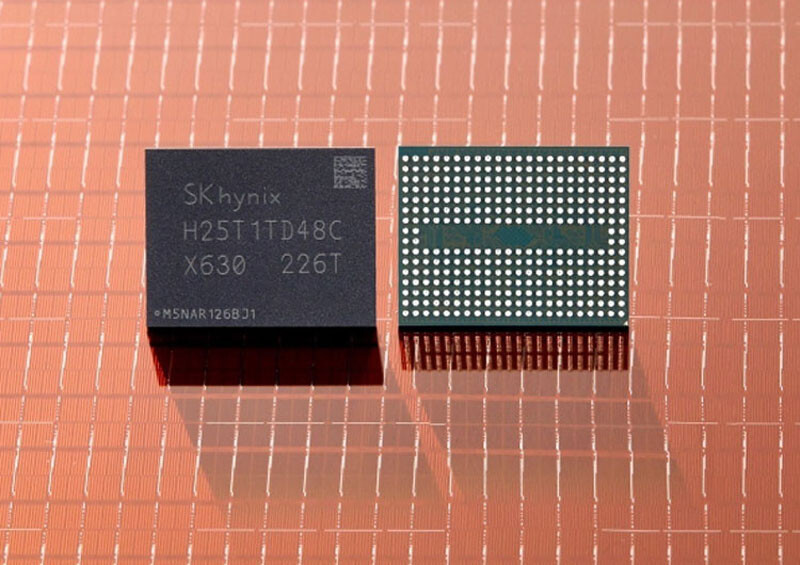
TrendForce points out that to meet the demand surge in the second half of the year, especially given Kioxia and Western Digital's currently low inventory, the production increase is mainly targeting 112-layer and select 2D products. This strategy is expected not only to secure profitability within the year but also to contribute to a projected 10.9% rise in the annual NAND Flash industry supply bit growth rate for 2024.

Balatro Sells a Million Copies in One Month

"Balatro," the latest indie game sensation published by Playstack has reached a significant milestone by selling one million copies in its first month. This achievement highlights the game's widespread appeal and the enthusiastic response from the gaming community. "We're incredibly grateful for the support and enthusiasm from players worldwide," says Harvey Elliott, CEO of Playstack. "The game's success is a testament to the quality and creativity that the indie sector can deliver, proving that even in uncertain times, innovative games can thrive. We extend our deepest thanks to every player who has joined us on this adventure."

LocalThunk, the solo developer behind "Balatro," shared their gratitude for the game's reception as well. "I'm so grateful to all the players and people that have made this happen. I still can't grasp the response to this game, and I am overjoyed that so many people have been able to have fun with my silly creation. I'm so fortunate that I can continue working on my passion as a career. Thank you!"

PS5 DualSense Controller Software Update Enhances Speaker & Mic Functionality

Update on March 13, 2024: the PS5 system software update is rolling out globally today. Additionally, later this month a PlayStation App update will enable users to enjoy Share Screen interactions on the app as well. As the new year kicks into high gear with an amazing slate of PS5 game releases like The Last of Us Part II Remastered, Tekken 8 and Helldivers 2, along with FINAL FANTASY VII Rebirth, we're pleased to roll out another PS5 system software beta today with a number of quality-of-life enhancements and new features.

While beta access is limited to invited participants in select countries, we plan to release the update globally in the coming months. If you're selected to participate in the beta, you'll receive an email invitation today when it's available to download. Some features available during the beta phase may not make it into the final version or may see significant changes. Let's jump in to the newly added features below.

"Outcast - A New Beginning" Director Discusses Open World Mechanics

Every choice we made when developing Outcast - A New Beginning had, at its core, one motivation: freedom. It was important to us not to limit where players could go at any point; instead, we gave them the tools to navigate the detailed open world we've spent the last few years crafting. We're incredibly proud of Outcast's world and want players to share its richness with us. As players set out across Adelpha, we want to reward them for their curiosity and sense of adventure. Whether it's blitzing through an invader base and unlocking a new weapon module, zipping through gliding challenges to earn jetpack upgrades, or simply taking in the sights, we've strived to make every second spent on the planet of Adelpha feel meaningful to players.

Traveling in style
Knowing that players would be spending a lot of time in Cutter Slade's boots, it was important to us that it felt fun to maneuver him through the world. Open-world games often ask players to cross great distances, and it's our job as developers to ensure that you always feel invigorated by navigating the wilds of Adelpha. When designing how Cutter moved through the world, we didn't want to gatekeep fun traversal abilities for later in the game. From early in Outcast - A New Beginning, you can take advantage of Adelpha's teetering precipices and deep valleys with your gliding suit, swooping across the alien landscape.

NVIDIA Cracks Down on CUDA Translation Layers, Changes Licensing Terms

NVIDIA's Compute Unified Device Architecture (CUDA) has long been the de facto standard programming interface for developing GPU-accelerated software. Over the years, NVIDIA has built an entire ecosystem around CUDA, cementing its position as the leading GPU computing and AI manufacturer. However, rivals AMD and Intel have been trying to make inroads with their own open API offerings—ROCm from AMD and oneAPI from Intel. The idea was that developers could more easily run existing CUDA code on non-NVIDIA GPUs by providing open access through translation layers. Developers had created projects like ZLUDA to translate CUDA to ROCm, and Intel's CUDA to SYCL aimed to do the same for oneAPI. However, with the release of CUDA 11.5, NVIDIA appears to have cracked down on these translation efforts by modifying its terms of use, according to developer Longhorn on X.

"You may not reverse engineer, decompile or disassemble any portion of the output generated using Software elements for the purpose of translating such output artifacts to target a non-NVIDIA platform," says the CUDA 11.5 terms of service document. The changes don't seem to be technical in nature but rather licensing restrictions. The impact remains to be seen, depending on how much code still requires translation versus running natively on each vendor's API. While CUDA gave NVIDIA a unique selling point, its supremacy has diminished as more libraries work across hardware. Still, the move could slow the adoption of AMD and Intel offerings by making it harder for developers to port existing CUDA applications. As GPU-accelerated computing grows in fields like AI, the battle for developer mindshare between NVIDIA, AMD, and Intel is heating up.

3D Nanoscale Petabit Capacity Optical Disk Format Proposed by Chinese R&D Teams

The University of Shanghai for Science and Technology (USST), Peking University and the Shanghai Institute of Optics and Fine Mechanics (SIOM) are collaborating on new Optical Data Storage (ODS) technologies—a recently published paper reveals that scientists are attempting to create 3D nanoscale optical disk memory that breaks into petabit capacities. Society (as a whole) has an ever-growing data demand—this requires the development of improved high-capacity storage technologies—the R&D teams believe that ODS presents a viable alternative route to traditional present day solutions: "data centers based on major storage technologies such as semiconductor flash devices and hard disk drives have high energy burdens, high operation costs and short lifespans."

The proposed ODS format could be a "promising solution for cost-effective long-term archival data storage." The researchers note that current (e.g Blu-ray) and previous generation ODS technologies have been: "limited by low capacities and the challenge of increasing areal density." In order to get ODS up to petabit capacity levels, several innovations are required—the Nature.com abstract stated: "extending the planar recording architecture to three dimensions with hundreds of layers, meanwhile breaking the optical diffraction limit barrier of the recorded spots. We develop an optical recording medium based on a photoresist film doped with aggregation-induced emission dye, which can be optically stimulated by femtosecond laser beams. This film is highly transparent and uniform, and the aggregation-induced emission phenomenon provides the storage mechanism. It can also be inhibited by another deactivating beam, resulting in a recording spot with a super-resolution scale." The novel optical storage medium relies on dye-doped photoresist (DDPR) with aggregation-induced emission luminogens (AIE-DDPR)—a 515 nm femtosecond Gaussian laser beam takes care of optical writing tasks, while a doughnut-shaped 639 nm continuous wave laser beam is tasked with retrieval. A 480 nm pulsed laser and a 592 nm continuous wave laser work in tandem to read data.

Groq LPU AI Inference Chip is Rivaling Major Players like NVIDIA, AMD, and Intel

AI workloads are split into two different categories: training and inference. While training requires large computing and memory capacity, access speeds are not a significant contributor; inference is another story. With inference, the AI model must run extremely fast to serve the end-user with as many tokens (words) as possible, hence giving the user answers to their prompts faster. An AI chip startup, Groq, which was in stealth mode for a long time, has been making major moves in providing ultra-fast inference speeds using its Language Processing Unit (LPU) designed for large language models (LLMs) like GPT, Llama, and Mistral LLMs. The Groq LPU is a single-core unit based on the Tensor-Streaming Processor (TSP) architecture which achieves 750 TOPS at INT8 and 188 TeraFLOPS at FP16, with 320x320 fused dot product matrix multiplication, in addition to 5,120 Vector ALUs.

Having massive concurrency with 80 TB/s of bandwidth, the Groq LPU has 230 MB capacity of local SRAM. All of this is working together to provide Groq with a fantastic performance, making waves over the past few days on the internet. Serving the Mixtral 8x7B model at 480 tokens per second, the Groq LPU is providing one of the leading inference numbers in the industry. In models like Llama 2 70B with 4096 token context length, Groq can serve 300 tokens/s, while in smaller Llama 2 7B with 2048 tokens of context, Groq LPU can output 750 tokens/s. According to the LLMPerf Leaderboard, the Groq LPU is beating the GPU-based cloud providers at inferencing LLMs Llama in configurations of anywhere from 7 to 70 billion parameters. In token throughput (output) and time to first token (latency), Groq is leading the pack, achieving the highest throughput and second lowest latency.

YMTC Develops 128 and 232-Layer Xtacking 4.0 NAND Memory Chips

Chinese memory maker Yangtze Memory Technology Corp (YMTC) is allegedly preparing its next-generation Xtacking 4.0 3D NAND flash architecture for next-generation memory chips. According to the documentation obtained by Tom's Hardware, YMTC has developed two SKUs based on the upgraded Xtacking 4.0: X4-9060, a 128-layer three-bit-per-cell (TLC) 3D NAND, and the X4-9070, a 232-layer TLC 3D NAND. By using string stacking on both of these SKUs, YMTC plans to make the 3D NAND work by incorporating arrays with 64 and 116 active layers stacked on top of each other. This way, the export regulation rules from the US government are met, and the company can use the tools that are not under the sanction list.

While YMTC has yet to fully disclose the specific advantages of the Xtacking 4.0 technology, the industry anticipates significant enhancements in data transfer speeds and storage density. These improvements are expected to stem from increased plane counts for optimized parallel processing, refined bit/word line configurations to minimize latency, and the development of modified chip variants to boost production yields. When YMTC announced Xtacking 3.0, the company offered 128-layer TLC and 232-layer four-bit-per-cell (QLC) variants and was the first company to achieve 200+ layer count in the 3D NAND space. The Xtacking 3.0 architecture incorporates string stacking and hybrid bonding techniques and uses a mature process node for the chip's CMOS underlayer. We have to wait for the final Xtacking 4.0 details when YMTC's officially launches the SKUs.

Samsung Electronics Holds Memory Tech Day 2023 Unveiling New Innovations To Lead the Hyperscale AI Era

Samsung Electronics Co., Ltd., a world leader in advanced memory technology, today held its annual Memory Tech Day, showcasing industry-first innovations and new memory products to accelerate technological advancements across future applications—including the cloud, edge devices and automotive vehicles.

Attended by about 600 customers, partners and industry experts, the event served as a platform for Samsung executives to expand on the company's vision for "Memory Reimagined," covering long-term plans to continue its memory technology leadership, outlook on market trends and sustainability goals. The company also presented new product innovations such as the HBM3E Shinebolt, LPDDR5X CAMM2 and Detachable AutoSSD.

Intel Unveils Industry-Leading Glass Substrates to Meet Demand for More Powerful Compute

What's New: Intel today announced one of the industry's first glass substrates for next-generation advanced packaging, planned for the latter part of this decade. This breakthrough achievement will enable the continued scaling of transistors in a package and advance Moore's Law to deliver data-centric applications.

"After a decade of research, Intel has achieved industry-leading glass substrates for advanced packaging. We look forward to delivering these cutting-edge technologies that will benefit our key players and foundry customers for decades to come."
-Babak Sabi, Intel senior vice president and general manager of Assembly and Test Development

UPMEM Raises €7M to Revolutionize AI and Analytics Processing

UPMEM, a fabless semiconductor startup has raised €4.1 M equity from the European Innovation Council (EIC) Fund and Venture Capitalists (Partech, Western Digital Capital, C4 Ventures…), and a €2.5M grant from the EIC. Founded by Fabrice Devaux and Gilles Hamou, the company is pioneering ultra-efficient Processing In Memory (PIM) accelerators to tackle the significant challenge of compute efficiency for AI and big data applications.

UPMEM's PIM solution, integrating UPMEM's first commercial-grade PIM chip on the market, is now available to cloud markets across the globe (US, Asia...) to provide the most cost-effective and energy-efficient solutions for AI and analytics applications in data centers and at the edge, such as large language models (LLM e.g. GPT), genomics, large analytics.

Samsung Electronics Unveils Industry's Highest-Capacity 12nm-Class 32Gb DDR5 DRAM

collaboration with diverse industries and support various applications
Samsung Electronics, a world leader in advanced memory technology, today announced that it has developed the industry's first and highest-capacity 32-gigabit (Gb) DDR5 DRAM using 12 nanometer (nm)-class process technology. This achievement comes after Samsung began mass production of its 12 nm-class 16Gb DDR5 DRAM in May 2023. It solidifies Samsung's leadership in next-generation DRAM technology and signals the next chapter of high-capacity memory.

"With our 12 nm-class 32Gb DRAM, we have secured a solution that will enable DRAM modules of up to 1-terabyte (TB), allowing us to be ideally positioned to serve the growing need for high-capacity DRAM in the era of AI (Artificial Intelligence) and big data," said SangJoon Hwang, Executive Vice President of DRAM Product & Technology at Samsung Electronics. "We will continue to develop DRAM solutions through differentiated process and design technologies to break the boundaries of memory technology."

Global Enterprise SSD Revenue Hits New Low in Q2 at US$1.5 Billion, Peak Season Growth Expected to Fall Short of Forecasts

TrendForce research reveals that, due to the impacts of high inflation and economic downturn, CSPs are adopting more conservative strategies when it comes to capital expenditure and consistently reducing their annual server demand forecasts. Currently, CSPs in China have reported a decline in cloud orders compared to last year, leading to a subsequent decrease in annual procurement volumes for enterprise SSDs. In North America, some clients have postponed mass production timelines for new server platforms while ramping up investments in AI servers. These factors have resulted in enterprise SSD orders falling below expectations. Consequently, global enterprise SSD revenue hit an all-time low in the second quarter, totaling just $1,500 million—a QoQ decrease of 24.9%.

Demand for AI servers remains strong in the third quarter, while orders and shipment momentum for general-purpose servers have yet to show signs of recovery. This continues to put pressure on the purchasing volume of enterprise SSDs, and annual bit volume is expected to be lower than last year. Meanwhile, vendors have once again reduced capacity utilization to slow down inventory growth. Server customers still maintain high inventory levels, and their purchasing momentum remains insufficient. This is expected to lead to an approximate 15% QoQ decline in the average price of enterprise SSDs in the third quarter, which may further result in a lackluster revenue performance for the peak season.

BBCube 3D Could be the Future of Stacked DRAM

Scientists at the Tokyo Institute of Technology have developed a new type of stacked or 3D DRAM that the researchers call Bumpless Build Cube 3D or BBCube 3D, which relies on Through Silicon Vias or TSVs to connect the DRAM dies. This is a different approach to HBM which relies on micro bumps to connect the layers together and the Japanese scientists are saying that their bumpless wafer-on-wafer solution should allow not only for an easier manufacturing process, but more importantly, improved cooling, as the TSVs can channel the heat from the DRAM dies down into whatever substrate the BBCube 3D stack is finally mounted onto.

If that wasn't enough, the researchers believe that BBCube 3D will be able to deliver higher speeds than HBM courtesy of a combination of the TSVs being relatively short and "high-density signal parallelism". BBCube 3D is expected to deliver up to a 32 fold increase in bandwidth compared to DDR5 memory and a four fold increase compared to HBM2E memory, while at the same time, drawing less power. The research paper goes into a lot more details for those interested at taking a closer look at this potentially revolutionary shift in DRAM assembly. However, the question that remains unanswered is if this will end up as a real world product some time in the near future, which is all based on how manufacturable BBCube 3D memory will be.

Intel to Demonstrate PowerVia on E-Core Processor Built with Intel 4 Node

At VLSI Symposium 2023, scheduled to take place between June 11-16, Intel is set to demonstrate its PowerVia technology working efficiently on an E-Core chip built using the Intel 4 node. Conventional chips have power and signal interconnects distributed across multiple metal layers. PowerVia, on the other hand, dedicates specific layers for power delivery, effectively separating them from the signal routing layers. This approach allows for vertical power delivery through a set of power-specific Through-Silicon Vias (TSVs) or PowerVias, which are essentially vertical connections between the top and bottom surfaces of the chip. By delivering power directly from the backside of the chip, PowerVia reduces power supply noise and resistive losses, optimizing power distribution and improving overall energy efficiency. PowerVia is set to make a debut in 2024 with Intel 20A node.

For VLSI Symposium 2023 talk, the company has prepared a paper that highlights a design made using Intel 4 technology and implements E-Cores only in a test chip. The document states: "PowerVia Technology is a novel innovation to extend Process Scaling by having Power Delivery on the backside. This paper presents the pre and post silicon findings from implementing an Intel E-Core in PowerVia Technology. PowerVia enabled standard cell utilization of greater than 90 percent in large areas of the core while showing greater than 5 percent frequency benefit in silicon due reduced IR drop. Successful Post silicon debug is demonstrated with slightly higher but acceptable throughput times. The thermal characteristics of the PowerVia testchip is inline with higher power densities expected from logic scaling."

MIT Researchers Grow Transistors on Top of Silicon Wafers

MIT researchers have developed a groundbreaking technology that allows for the growth of 2D transition metal dichalcogenide (TMD) materials directly on fully fabricated silicon chips, enabling denser integrations. Conventional methods require temperatures of about 600°C, which can damage silicon transistors and circuits as they break down above 400°C. The MIT team overcame this challenge by creating a low-temperature growth process that preserves the chip's integrity, allowing 2D semiconductor transistors to be directly integrated on top of standard silicon circuits. The new approach grows a smooth, highly uniform layer across an entire 8-inch wafer, unlike previous methods that involved growing 2D materials elsewhere before transferring them to a chip or wafer. This process often led to imperfections that negatively impacted device and chip performance.

Additionally, the novel technology can grow a uniform layer of TMD material in less than an hour over 8-inch wafers, a significant improvement from previous methods that required over a day for a single layer. The enhanced speed and uniformity of this technology make it suitable for commercial applications, where 8-inch or larger wafers are essential. The researchers focused on molybdenum disulfide, a flexible, transparent 2D material with powerful electronic and photonic properties ideal for semiconductor transistors. They designed a new furnace for the metal-organic chemical vapor deposition process, which has separate low and high-temperature regions. The silicon wafer is placed in the low-temperature region while vaporized molybdenum and sulfur precursors flow into the furnace. Molybdenum remains in the low-temperature region, while the sulfur precursor decomposes in the high-temperature region before flowing back into the low-temperature region to grow molybdenum disulfide on the wafer surface.

SK Hynix Eighth-Generation 300-Layer 3D NAND is a World First, Breaks Bandwidth Records

SK Hynix representatives unveiled the company's latest breakthrough in 3D NAND development at the ISSCC 2023 conference. Details of a new flash memory prototype featuring over 300 layers were revealed, and the company stated that a team of 35 engineers had contributed to the presentation material. In order to highlight the boost in performance offered by the prototype's improvements, it was compared to SK Hynix's previous record holding seventh-generation 238-layer 3D NAND. The new eighth-generation 3D NAND posted bandwidth figures with a maximum of 194 MB/s, which contrasts favorably with the older model's rate of 164 MB/s, representing an 18% increase in performance.

Recording density also benefits from the 300+ active layer design, with SK Hynix mentioning a 1 Tb (128 GB) capacity with triple level cells and a bit density of over 20 GB/mm^2. The chip features a 16 KB page size, four planes and a 2400 MT/s interface. The increase in density will result in a lower per-Tb cost during the manufacturing process. It is hoped that the end consumer will ultimately benefit from the boost in performance and capacity.
Return to Keyword Browsing
Apr 29th, 2024 19:21 EDT change timezone

New Forum Posts

Popular Reviews

Controversial News Posts