Monday, September 18th 2023

Intel Unveils Industry-Leading Glass Substrates to Meet Demand for More Powerful Compute
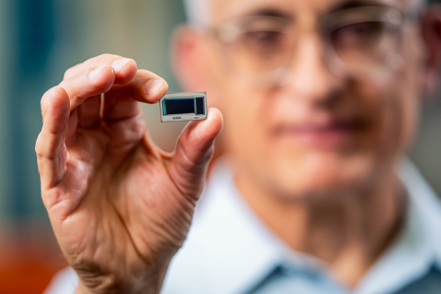
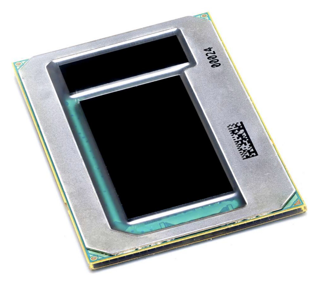
What's New: Intel today announced one of the industry's first glass substrates for next-generation advanced packaging, planned for the latter part of this decade. This breakthrough achievement will enable the continued scaling of transistors in a package and advance Moore's Law to deliver data-centric applications.
"After a decade of research, Intel has achieved industry-leading glass substrates for advanced packaging. We look forward to delivering these cutting-edge technologies that will benefit our key players and foundry customers for decades to come."
-Babak Sabi, Intel senior vice president and general manager of Assembly and Test Development


 Why It Matters: Compared to today's organic substrates, glass offers distinctive properties such as ultra-low flatness and better thermal and mechanical stability, resulting in much higher interconnect density in a substrate. These benefits will allow chip architects to create high-density, high-performance chip packages for data-intensive workloads such as artificial intelligence (AI). Intel is on track to deliver complete glass substrate solutions to the market in the second half of this decade, allowing the industry to continue advancing Moore's Law beyond 2030.
By the end of the decade, the semiconductor industry will likely reach its limits on being able to scale transistors on a silicon package using organic materials, which use more power and include limitations like shrinkage and warping. Scaling is crucial to the progress and evolution of the semiconductor industry, and glass substrates are a viable and essential next step for the next generation of semiconductors.
How It Works: As the demand for more powerful computing increases and the semiconductor industry moves into the heterogeneous era that uses multiple "chiplets" in a package, improvements in signaling speed, power delivery, design rules and stability of package substrates will be essential. Glass substrates possess superior mechanical, physical and optical properties that allow for more transistors to be connected in a package, providing better scaling and enabling assembly of larger chiplet complexes (called "system-in-package") compared to organic substrates in use today. Chip architects will have the ability to pack more tiles - also called chiplets - in a smaller footprint on one package, while achieving performance and density gains with greater flexibility and lower overall cost and power usage.
About the Use Cases: Glass substrates will initially be introduced into the market where they can be leveraged the most: applications and workloads requiring larger form factor packages (i.e., data centers, AI, graphics) and higher speed capabilities.
Glass substrates can tolerate higher temperatures, offer 50% less pattern distortion, and have ultra-low flatness for improved depth of focus for lithography, and have the dimensional stability needed for extremely tight layer-to-layer interconnect overlay. As a result of these distinctive properties, a 10x increase in interconnect density is possible on glass substrates. Further, improved mechanical properties of glass enable ultra-large form-factor packages with very high assembly yields.
Glass substrates' tolerance to higher temperatures also offers chip architects flexibility on how to set the design rules for power delivery and signal routing because it gives them the ability to seamlessly integrate optical interconnects, as well as embed inductors and capacitors into the glass at higher temperature processing. This allows for better power delivery solutions while achieving high-speed signaling that is needed at much lower power. These many benefits bring the industry closer to being able to scale 1 trillion transistors on a package by 2030.
How We Do It: Intel has been researching and evaluating the reliability of glass substrates as a replacement for organic substrates for more than a decade. The company has a long history of enabling next-generation packaging, having led the industry in the transition from ceramic package to organic package in the 1990s, being the first to enable halogen and lead-free packages, and being the inventor of advanced embedded die packaging technologies, the industry's first active 3D stacking technologies. As a result, Intel has been able to unlock an entire ecosystem around these technologies from equipment, chemical and materials suppliers to substrate manufacturers.
What's Next: Building on the momentum of recent PowerVia and RibbonFET breakthroughs, these industry-leading glass substrates for advanced packaging demonstrate Intel's forward focus and vision for the next era of compute beyond the Intel 18A process node. Intel is on the path to delivering 1 trillion transistors on a package by 2030 and its ongoing innovation in advanced packaging including glass substrates will help achieve this goal.
Source:
Intel
"After a decade of research, Intel has achieved industry-leading glass substrates for advanced packaging. We look forward to delivering these cutting-edge technologies that will benefit our key players and foundry customers for decades to come."
-Babak Sabi, Intel senior vice president and general manager of Assembly and Test Development


By the end of the decade, the semiconductor industry will likely reach its limits on being able to scale transistors on a silicon package using organic materials, which use more power and include limitations like shrinkage and warping. Scaling is crucial to the progress and evolution of the semiconductor industry, and glass substrates are a viable and essential next step for the next generation of semiconductors.
How It Works: As the demand for more powerful computing increases and the semiconductor industry moves into the heterogeneous era that uses multiple "chiplets" in a package, improvements in signaling speed, power delivery, design rules and stability of package substrates will be essential. Glass substrates possess superior mechanical, physical and optical properties that allow for more transistors to be connected in a package, providing better scaling and enabling assembly of larger chiplet complexes (called "system-in-package") compared to organic substrates in use today. Chip architects will have the ability to pack more tiles - also called chiplets - in a smaller footprint on one package, while achieving performance and density gains with greater flexibility and lower overall cost and power usage.
About the Use Cases: Glass substrates will initially be introduced into the market where they can be leveraged the most: applications and workloads requiring larger form factor packages (i.e., data centers, AI, graphics) and higher speed capabilities.
Glass substrates can tolerate higher temperatures, offer 50% less pattern distortion, and have ultra-low flatness for improved depth of focus for lithography, and have the dimensional stability needed for extremely tight layer-to-layer interconnect overlay. As a result of these distinctive properties, a 10x increase in interconnect density is possible on glass substrates. Further, improved mechanical properties of glass enable ultra-large form-factor packages with very high assembly yields.
Glass substrates' tolerance to higher temperatures also offers chip architects flexibility on how to set the design rules for power delivery and signal routing because it gives them the ability to seamlessly integrate optical interconnects, as well as embed inductors and capacitors into the glass at higher temperature processing. This allows for better power delivery solutions while achieving high-speed signaling that is needed at much lower power. These many benefits bring the industry closer to being able to scale 1 trillion transistors on a package by 2030.
How We Do It: Intel has been researching and evaluating the reliability of glass substrates as a replacement for organic substrates for more than a decade. The company has a long history of enabling next-generation packaging, having led the industry in the transition from ceramic package to organic package in the 1990s, being the first to enable halogen and lead-free packages, and being the inventor of advanced embedded die packaging technologies, the industry's first active 3D stacking technologies. As a result, Intel has been able to unlock an entire ecosystem around these technologies from equipment, chemical and materials suppliers to substrate manufacturers.
What's Next: Building on the momentum of recent PowerVia and RibbonFET breakthroughs, these industry-leading glass substrates for advanced packaging demonstrate Intel's forward focus and vision for the next era of compute beyond the Intel 18A process node. Intel is on the path to delivering 1 trillion transistors on a package by 2030 and its ongoing innovation in advanced packaging including glass substrates will help achieve this goal.
7 Comments on Intel Unveils Industry-Leading Glass Substrates to Meet Demand for More Powerful Compute
Using words in quotes like ‘chiplets’ in its press release seems like Intel is extending an olive branch.
Maybe chiplets and tiles are the same thing - but what Intel calls them depends on who makes the glue between them?
en.m.wikipedia.org/wiki/List_of_semiconductor_fabrication_plants
TSMC has demonstrated that the big money is in the big chips. Intel will need these customers if it will ever make a play as a foundry partner. I just don’t see it if Intel continues to go head to head with competing big chips.